GOWIN IPUG800-1.0E Receiver IP
Contents
IMPORTANT INFORMATION
Copyright © 2022 Guangdong Gowin Semiconductor Corporation. All Rights Reserved.
 is a trademark of Guangdong Gowin Semiconductor Corporation and is registered in China, the U.S. Patent and Trademark Office, and other countries. All other words and logos identified as trademarks or service marks are the property of their respective holders. No part of this document may be reproduced or transmitted in any form or by any denotes, electronic, mechanical, photocopying, recording or otherwise, without the prior written consent of GOWINSEMI.
Disclaimer
GOWINSEMI assumes no liability and provides no warranty (either expressed or implied) and is not responsible for any damage incurred to your hardware, software, data, or property resulting from usage of the materials or intellectual property except as outlined in the GOWINSEMI Terms and Conditions of Sale. GOWINSEMI may make changes to this document at any time without prior notice. Anyone relying on this documentation should contact GOWINSEMI for the current documentation and errata.
Revision History
| Date | Version | Description |
| 08/17/2022 | 1.0E | Initial version published. |
About This Guide
Purpose
The purpose of Gowin NPU IP User Guide is to help you quickly learn the features and usage of Gowin NPU IP by providing the descriptions of functions, signal definitions, parameters, GUI, and reference design, etc.
Supported Products
The information in this guide applies to the following product: GW2AR-18C QFN88P.
Related Documents
You can find the related documents at GOWINSEMI website: www.gowinsemi.com.
- DS226, GW2AR series of FPGA Products Data Sheet
- SUG100, Gowin Software User Guide
- SUG549, MCU Designer User Guide.
Terminology and Abbreviation
Table 1-1 shows the abbreviations and terminology used in this manual.
Table 1-1 Terminology and Abbreviations
| Terminology and Abbreviations | Meaning |
| NPU | Neural-network Processing Unit |
| AI | Artificial Intelligence |
| PSRAM | Pseudo Static Random Access Memory |
| SPI | Serial Peripheral Interface |
| AHB | Advanced High Performance Bus |
| MJB | Magic Jelly Bean |
| FPGA | Field Programmable Gate Array |
| MCU | Microcontroller Unit |
| IP | Intellectual Property |
| DVI | Digital Visual Interface |
| PC | Personal Computer |
Support and Feedback
Gowin Semiconductor provides customers with comprehensive technical support. If you have any questions, comments, or suggestions, please feel free to contact us directly by the following ways.
Website: www.gowinsemi.com
E-mail: [email protected]
Overview
Overview
Gowin NPU IP, embedded neural-network processing unit, is used to accelerate the parallel computing of machine learning algorithms, including AHB bridge unit, accelerator unit, PSRAM controller unit, and SPI Flash controller unit.
AHB bridge unit, which is bridged with MCU through AHB bus, is used to realize the cooperative work between NPU and MCU.
Accelerator unit invokes machine learning algorithms and accelerates the parallel computing of AI models. The machine learning algorithms supported by the accelerator unit include the depth wise convolution algorithm (DepthwiseConv2D), the two-dimensional convolution algorithm (Conv2D), the maximum pooling algorithm (MaxPool2D), and the average pooling algorithm (AveragePool2D).
PSRAM controller unit assists accelerator unit in storing temporary calculation data. When the accelerator unit computes the AI model of each layer, PSRAM inputs the data from the previous layer of the model, and outputs the data of the current layer to the next layer after the current layer computation is completed.
The SPI Flash controller unit assists accelerator unit in storing the weight data and bias data of AI model. When the accelerator unit computes the AI model of each layer, it reads model weight data and bias data of the current layer from the SPI Flash to compute the machine learning algorithm of the current layer.
Features
The features of Gowin NPU IP include:
- Support AHB bridge to work with MCU
- Invoke machine learning algorithms to accelerate the computation of AI models in parallel
- Embedded PSRAM controller unit
- Embedded SPI Flash controller unit
Functional Description
Structure
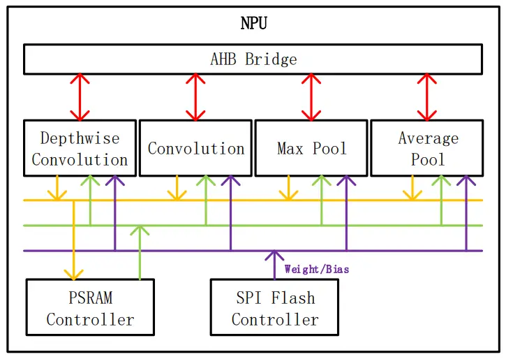
Gowin NPU IP includes AHB bridge unit, accelerator unit, PSRAM controller unit, and SPI Flash controller unit as shown in Figure 3-1.
Figure 3-1 NPU Structure
Function
AHB Bridge Unit
AHB Bridge Unit is the front-end input interface unit that bridges with the MCU.
After parsing an AI model, the parameter, weight, and bias data of the model are extracted. MCU controls the parameter data and target data (e.g., image data), which are input to the accelerator unit through AHB bridge unit of the NPU to compute the machine learning algorithms of each layer of the model.
Accelerator Unit
Accelerator unit is used to invoke the machine learning algorithm and accelerate the parallel computing of each layer of AI models. For example, if a layer of the AI model is a depth wise convolutional layer, the accelerator unit invokes the depth wise convolutional algorithm to compute this layer. The accelerator unit includes the depth wise convolution algorithm (DepthwiseConv2D), the two-dimensional convolution algorithm (Conv2D), the maximum pooling algorithm (MaxPool2D), and the average pooling algorithm (AveragePool2D), etc.
PSRAM Controller Unit
When the accelerator unit computes a layer of the AI model, PSRAM controller unit controls the output data of the previous layer of the model and inputs it to the current layer as the input data of the current layer of the model. After the computation of the model current layer, the computation data is output to the next layer as the input data of the next layer.
SPI Flash Controller Unit
SPI Flash controller unit controls reading the weight data and bias data of the current layer from SPI Flash when the accelerator unit computes a layer of the AI model to compute machine learning algorithm of the current layer.
Port List
The ports of Gowin NPU IP are shown in Table 4-1.
Table 4-1 Gowin NPU IP Port List
| No. | Signal Name | Bit Width | I/O | Description |
| 1 | pri_fclk | 1 | input | PSRAM fast clock signal |
| 2 | pri_fclk90 | 1 | input | pri_fclk 90 degree phase clock |
| 3 | O_psram_ck | [1:0] | output | A clock signal provided to PSRAM |
| 4 | O_psram_ck_n | [1:0] | output | Compose the differential signal with the O_psram_ck |
| 5 | IO_psram_rwds | [1:0] | inout | PSRAM data strobe signal and mask signal |
| 6 | IO_psram_dq | [15:0] | inout | PSRAM data |
| 7 | O_psram_reset_n | [1:0] | output | PSRAM reset, active-low. |
| 8 | O_psram_cs_n | [1:0] | output | PSRAM chip selected |
| 9 | spi_io | [3:0] | inout | SPI Flash input/output data, reset, reference clock |
| 10 | spi_clk | 1 | output | SPI Flash clock signal |
| 11 | spi_cs_n | 1 | output | SPI-Flash chip selected |
| 12 | HCLK | 1 | input | AHB bus working clock signal |
| 13 | HRESETn | 1 | input | AHB bus reset, active-low |
| 14 | HSELS | 1 | input | AHB bus slave selection signal |
| 15 | HADDRS | [11:0] | input | AHB bus address |
| 16 | HTRANSS | [1:0] | input | AHB bus transfer type |
| 17 | HSIZES | [2:0] | input | AHB bus transfer size |
| 18 | HWRITES | 1 | input | AHB bus read/write signal:1 for write, 0 for read. |
| 19 | HREADYS | 1 | input | AHB bus master ready signal |
| 20 | HWDATAS | [31:0] | input | AHB bus write data |
| 21 | HREADYOUTS | 1 | output | AHB bus slave ready signal |
| 22 | HRESPS | 1 | output | AHB bus transfer response |
| 23 | HRDATAS | [31:0] | output | AHB bus read data |
Interface Configuration
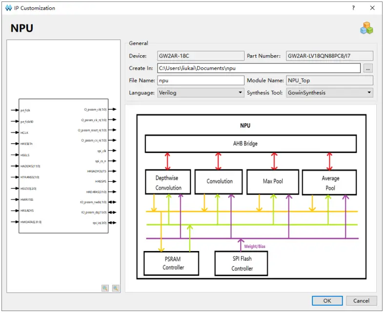
You can invoke and generate Gowin NPU IP through the IP Core Generator tool of Gowin Software (Education Version). Gowin NPU IP interface configuration is as shown in Figure 5-1. Click “OK” to generate Gowin NPU IP.
Figure 5-1 Gowin NPU IP Interface Configuration
Reference Design
Structure
To facilitate you to quickly get familiar with and use Gowin NPU IP, a reference design is provided to realize person and object detection and recognition. The block diagram of reference design is as shown in Figure 6-1.
Figure 6-1 Block Diagram of Reference Design
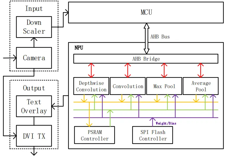
In the reference design, the following subsystems are included: Front-end input subsystem (Input): Camera acquires image data, and the raw image data is processed by image reduction (Down Scaler) to 96×96, which is input to NPU through MCU (AHB Bus) as NPU input data.
MCU subsystem: Works with NPU to control image data, AI model
parameter data, AI model operation data, weight data and bias data to interact with NPU.
NPU subsystem: Invokes machine learning algorithms and accelerates the parallel computing of AI models.
Back-end output subsystem: Compares the final computation results of NPU, and outputs the text “Person” if the score of person is greater than the score of no person. Digital Video Interface (DVI TX): Outputs the text “Person” and displays the image on the monitor.
Development Kit
System Environment
- Window 7/10 (32 bits/64 bits)
- macOS 11.2.3
Development Board
MJB V1.2 Board:GW2AR-LV18QN88PC8/I7
Software
- FPGA Software: Gowin_V1.9.8.07 Education
- MCU Software: GMD_V1.1
- AI Software: MJB_V1.0.0
Verification
- Step 1: Synthesize and PnR NPU hardware reference design, or generate NPU using IP Core Generator of Gowin Software (Education Version) and insert user design to generate fs file and posp file.
- Step 2: If your PC does not have MJB software, please contact Gowin to obtain Windows or Macos MJB software to install.
- Step 3: Copy the fs file and posp file generated by Step 1 to the installed path of MJB software (such as USER_PATHMJBMJB_V1.0.0dataprojectsmjb_std_boardperson_d etectiondatafpga).
- Step 4: Open the MJB software and create a new MJB project by clicking “MJB STD Board > Person Detection > Camera”.
- Step 5: Connect the PC and MJB V1.2 Board through the download cable.
- Step 6: Connect the MJB V1.2 Board and the monitor through HDMI cable.
- Step 7: Run the MJB project, verify and test on board level. Note!
For Step 2 ~ Step 7, see MUG100, MJB Software User Guide.
File Delivery
The delivery file of Gowin NPU IP includes documentation and reference design.
Documents
Download or view the user guide online on the Gowin website.
Table 7-1 Document List
| Name | Description |
| IPUG800, Gowin NPU IP User Guide | Gowin NPU IP user guide, namely this one. |
| RN800, Gowin NPU IP Release Note | Gowin NPU IP release note |
Reference Design
NPU_RefDesign_V1.0RefDesign folder contains FPGA RTL hardware reference design project and MCU C software reference design project of Gowin NPU IP.
- FPGA_RefDesign: FPGA RTL hardware reference design project
- MCU_RefDesign: MCU C software reference design project Table 7-2 lists the FPGA RTL hardware reference design folder.
Table 7-2 Hardware Reference Design Folder List
| Name | Description |
| mjb_npu.v | The top module of reference design |
| colorbar_generator.v | Colorbar generator module |
| DVI_out.v | Digital visual interface output module |
| text_overlay.v | Text overlay module |
| downscaler.v | Image downscaler module |
| mjb_npu.cst | NPU physical constraints file |
| gowin_empu_m1 | Gowin_EMPU_M1 project folder |
| npu | NPU IP project folder |
| gowin_rpll | rPLL project folder |