ANALOG DEVICES ADMFM2000 Dual Channel Microwave Downconverter

Contents
FEATURES
- Full featured evaluation board for the ADMFM2000
- Operation control via the SDP-B board
- 6.0 V single-supply operation
EVALUATION KIT CONTENTS
- ADMFM2000-EVALZ evaluation board
ADDITIONAL HARDWARE REQUIRED
- 2 RF signal generators operating ≥32 GHz
- RF spectrum analyzer capable of measuring ≥8 GHz
- Network analyzer ≥32 GHz (optional for S-parameters)
- DC power supply (6 V/5 A)
- SDP-B controller board
- PC with Windows operating system and a USB 2.0 port (USB 1.1 compatible)
ADDITIONAL SOFTWARE REQUIRED
- ADMFM2000-EVALZ graphical user interface (GUI)
- SDP-B driver
EVALUATION BOARD PHOTOGRAPH
Figure 1. ADMFM2000-EVALZ Evaluation Board
GENERAL DESCRIPTION
The ADMFM2000 is a dual microwave downconverter with input RF and local oscillator (LO) frequency ranges covering 5 GHz to 32 GHz and an output intermediate frequency (IF) frequency range from 0.5 GHz to 8 GHz. A common LO input signal is split to feed two separate buffer amplifiers to drive the mixer in each channel. Each down conversion path consists of an low noise amplifier (LNA), a mixer, an IF filter, a digital step attenuator (DSA), and an IF amplifier.
The ADMFM2000-EVALZ is fabricated using FR-370HR, Rogers 4350 in 6 layers.
This user guide describes the ADMFM2000-EVALZ and the control software used to test the ADMFM2000. The ADMFM2000 data sheet provides additional information and must be consulted when using the ADMFM2000-EVALZ.
EVALUATION BOARD HARDWARE
The ADMFM2000-EVALZ provides the external components needed to operate the ADMFM2000 in various modes and configurations.
The SDP connector allows the user to communicate with the internal switch and DSA of the ADMFM2000 via a USB port on a Windows® -based PC.
The ADMFM2000-EVALZ requires the use of an SDP-B board along with the ADMFM2000-EVALZ GUI software to program the device. The SDP USB driver is available for download at www.analog.com/SDP-B. Follow the steps in the Installing the ADMFM2000- EVALZ GUI section to contact Analog Devices, Inc., to receive the ADMFM2000-EVALZ GUI installer.
POWER SUPPLY
The ADMFM2000-EVALZ requires a single 6.0 V DC power supply.
RF INPUT AND IF OUTPUT CONNECTIONS
The ADMFM2000-EVALZ has 11 edge-mounted RF connectors, which are described in Table 1.
ADMFM2000 MODES OF OPERATION
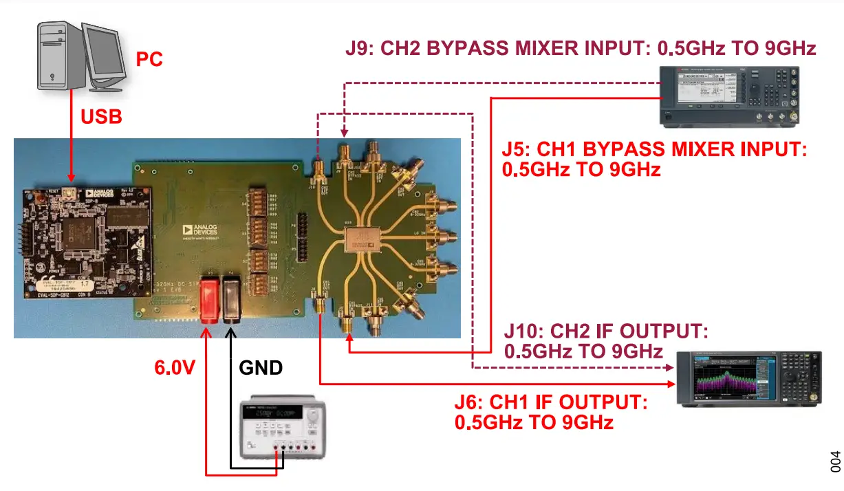
The three operating modes of the ADMFM2000-EVALZ are LNA only, mixer only, or mixer bypass (see Table 1 for further details). In addition, the LNA can be cascaded with the mixer (with an optional attenuation or filtering in between) by making a connection between the BPF IN and BPF OUT connectors. Refer to Figure 2 through Figure 4 for the hardware setup for each mode.
Table 1. Connectors
| Mode | Connector(s) | Name(s) | Input or Output | Description |
| LNA | J2 J3 J7 J8 | CH1 CH2 CH1 BPF OUT CH2 BPF OUT |
Input Input Output Output |
Channel 1 RF IN (LNA input) Channel 2 RF IN (LNA input) Channel 1 LNA output and input to the external band-pass filter (BPF) Channel LNA output and input to the external BPF |
| Mixer | J11 J12 J4 | CH1 BPF IN CH2 BPF IN LO IN | Input Input Input |
Channel 1 mixer input Channel 2 mixer input LO input for Channel 1 and Channel 2 |
| Mixer Bypass | J5 J9 |
CH1 BYPASS IN CH2 BYPASS IN |
Input Input |
Channel 1 mixer bypass input Channel 2 mixer bypass input |
| Mixer and Mixer Bypass | J6 J10 |
CH1 IF OUT CH2 IF OUT |
Output Output |
Channel 1 IF output, mixer, and mixer bypass mode Channel 2 IF output, mixer, and mixer bypass mode |
Figure 2. LNA Measurement Setup

Figure 3. Mixer Measurement Setup

Figure 4. Mixer Bypass Measurement Setup
EVALUATION BOARD SOFTWARE
The ADMFM2000 on the ADMFM2000-EVALZ can be programmed using the SDP-B controller board using a USB interface on a standard Windows PC.
SOFTWARE REQUIREMENTS AND INSTALLATION
Connect a Windows-based PC to the USB port of the SDP-B controller board to allow programming of the ADMFM2000-EVALZ using the GUI software, which is provided for download by Analog Devices once a software request form is submitted at https://form.analog.com/form_pages/softwaremodules/SRF.aspx.
For additional information on this software, see the Installing the ADMFM2000-EVALZ GUI section.
INSTALLING THE SDP-B USB DRIVER
To install the SDP USB driver, take the following steps:
- Download the SDP USB Driver Installer from the SDP-B product page.
- Open the downloaded file to begin the installation process. The default installation path is C:Program Files/Analog Devices/ SDPDriversR2.
INSTALLING THE ADMFM2000-EVALZ GUI
To install the ADMFM2000-EVALZ GUI software, take the following steps:
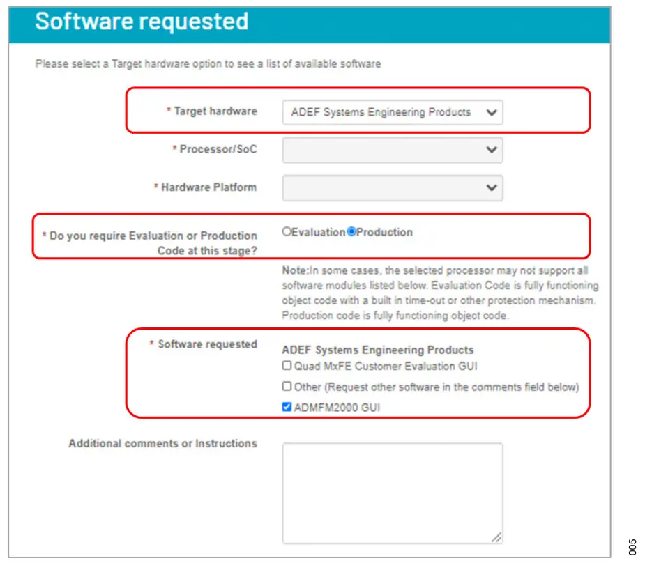
- Request the ADMFM2000 GUI software by filling out the software request form at: https://form.analog.com/form_pages/softwaremodules/SRF.aspx.
a. Note that a myAnalog account is required to access the form.
b. Fill out the form and submit it with the following options selected, as shown in Figure 5.
Figure 5. Software Request Form
- An email is then sent to the requester for downloading the software from the Analog Devices secure software distribution server. Once the software is downloaded, take the following steps:
a. Unzip the downloaded installer, ADEF_2_to_32GHz_Downconverter_SiP_GUI_Installer.zip.
b. Go to the unzipped folder, double-click on the installer file, ADEF_2_to_32GHz_Downconverter_SiP_GUI_Installer.exe and then follow the installation instructions on screen. Note that the default installation path is C:Program Files/ADEF_2_to_32GHz_Downconverter_SiP_GUI.
c. Ensure that the ADEF_2_to_32GHz_Downconverter_SiP_GUI.exe is located inside the C:Program Files/ ADEF_2_to_32GHz_Downconverter_SiP_GUI folder.
ADMFM2000-EVALZ CONNECTION
Take the following steps to connect the ADMFM2000-EVALZ:
- Set up the test hardware configuration for the desired operating mode, as shown in Figure 2, Figure 3, or Figure 4. Make sure the S1 switch on the secondary side of the ADMFM2000- EVALZ is flipped to the position shown of the S1 silkscreen.
- Power up the ADMFM2000-EVALZ and connect the USB cable to the PC and to the SDP-B controller board mounted onto the ADMFM2000-EVALZ.
- Power on the signal generator.
- Double-click the ADEF_2_to_32GHz_Downconverter_SiP_GUI shortcut on the desktop of the PC (if created) or the Start/ADEF_2_to_32GHz_Downconverter_SiP_GUI shortcut.
- The software opens the GUI view as shown in Figure 6.
Figure 6. GUI View When Running the ADEF_2_to_32GHz_Downconverter_SiP_GUI

- Click Connect Board, as shown in Figure 6 (Label A), and wait until it connects to the ADMFM2000-EVALZ and the Board Status: changes to Connected!, as shown in Figure 7.
Figure 7. GUI View Once Software Has Connected to the ADMFM2000- EVALZ
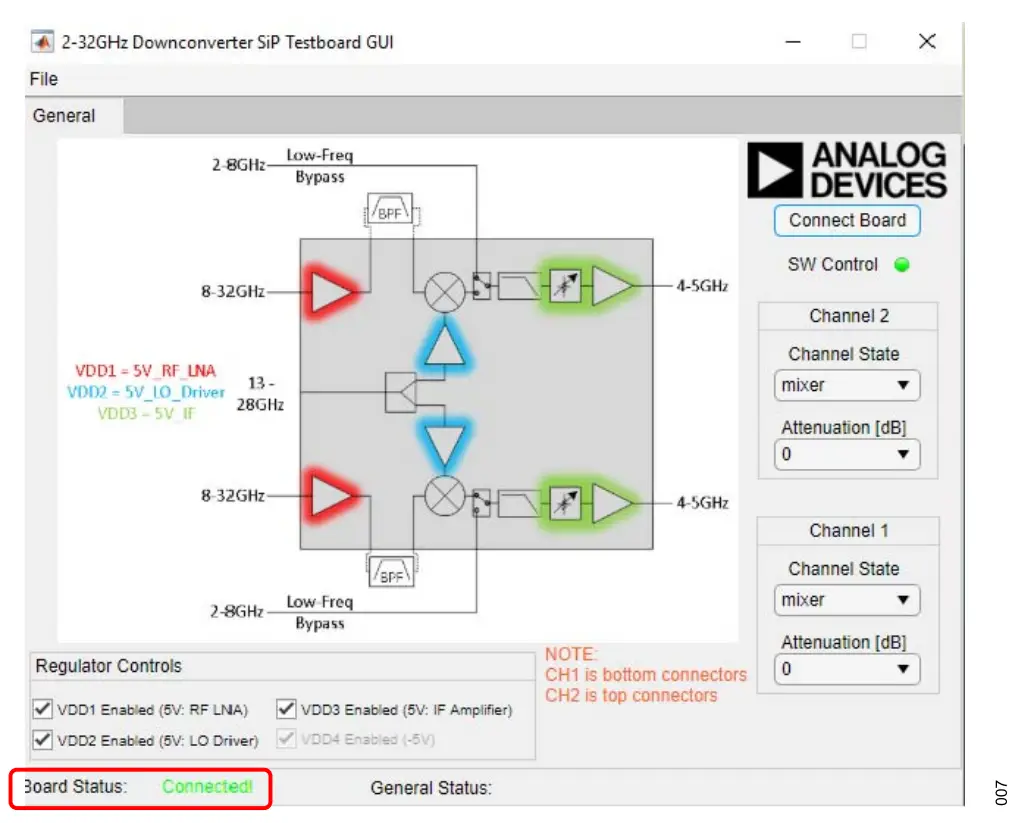
- If Board Status: shows Disconnected, unplug and relog the USB cable to the PC, and repeat Step 4 to Step 6.
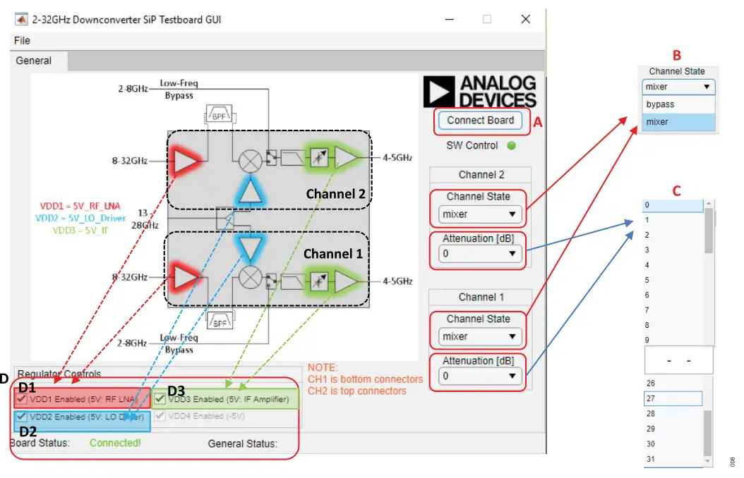
Figure 8. ADMFM2000 GUI Block Diagram
THE PROGRAMMING SEQUENCE TO SET THE MODE
To set the mode, follow this programming sequence:
- Run the ADMFM2000-EVALZ GUI software, as explained in the Installing the ADMFM2000-EVALZ GUI section.
- Click Connect Board (Label A, see Figure 8).
- Select and adjust from the dropdown menus in the Channel State (Label B), Attenuation [dB] (Label C), and Regulator Controls (Label D), respectively, as shown in Figure 8, if necessary.
- The updates are applied to the ADMFM2000 after selecting and adjusting is completed as directed in Step 3 in the ADMFM2000 GUI software.
Table 2. ADMFM2000 GUI Block Diagram User Inputs
| Label | Function |
| A | Click Connect Board to apply the configuration after any changes are made to the Channel State (Label B), Attenuation [dB] (Label C), and Regulator Controls (Label D). |
| B | The Channel State dropdown menu is where users select between mixer mode and bypass (mixer) mode. The mode must match the hardware setup shown in either Figure 3 and Figure 4. |
| C | The Channel x Attenuation [dB] dropdown menus allows users to set the DSA attenuation on Channel 1 or Channel 2, respectively. |
| D | The Regulator Controls allow users to enable or disable VDD1 or VDD2 on the amplifier (LNA, LO driver, and IF amplifier) in the signal path. |
| D1 | The VDD1 Enabled (5V: RF LNA) for both the Channel 1 and Channel 2 enable checkbox. |
| D2 | The VDD2 Enabled (5V: LO Driver) for both the Channel 1 and Channel 2 enable checkbox. |
| D3 | The VDD3 Enabled (5V: IF Amplifier) for both the Channel 1 and Channel 2 enable checkbox. |
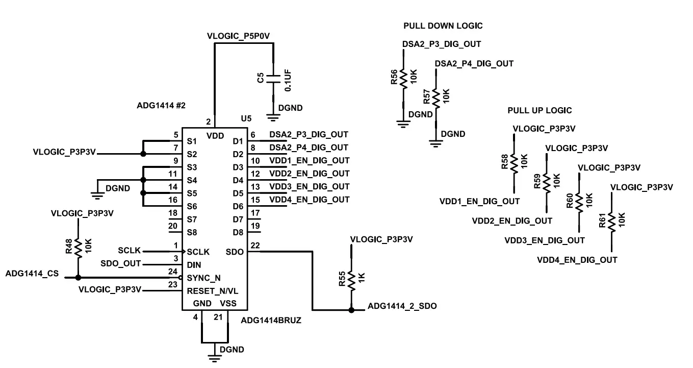
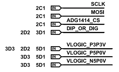
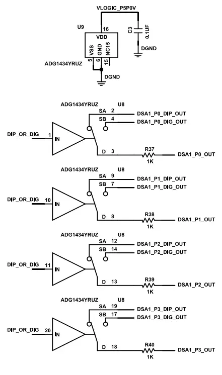
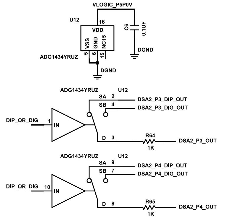
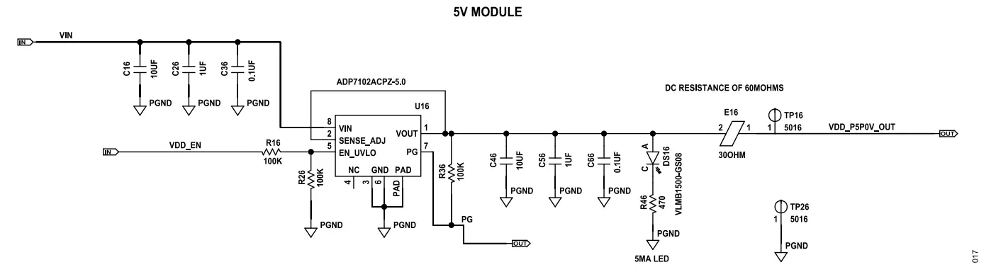
EVALUATION BOARD SCHEMATICS
DSA AND LDO ENABLE CONTROLS

SIP RF SW CONTROLS

IN SIGNALS
IN SIGNALS
OUT SIGNALS
IN SIGNALS
OUT SIGNALS

IN SIGNALS
OUT SIGNALS

IN SIGNALS
OUT SIGNALS
MUX FOR LDO ENABLES
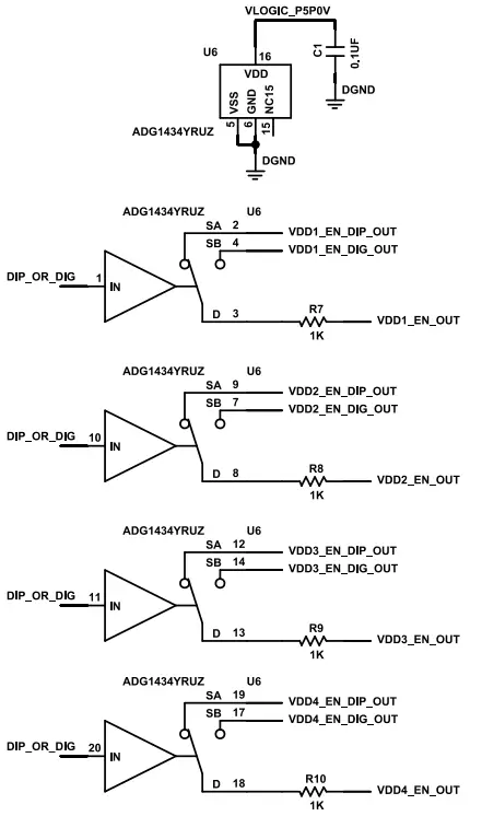
MUX FOR DSA1 CONTROLS
MUX FOR DSA1/2 CONTROLS

MUX FOR DSA2 CONTROLS
MUX FOR RF SWITCH CONTROLS
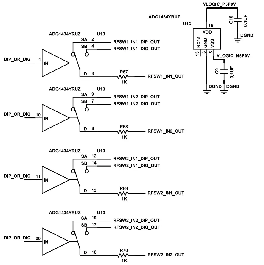
Figure 9. Control Circuit
Figure 10. SDP Interface
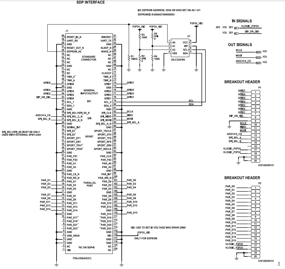
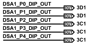
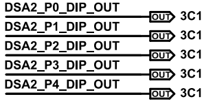
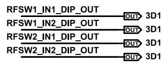
Figure 11. Dual Inline Package (DIP) Switches
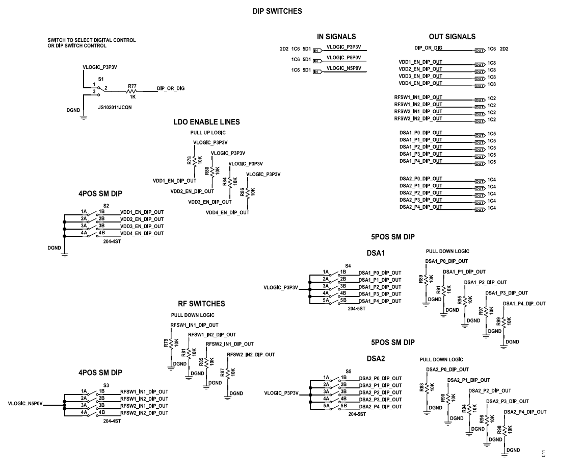
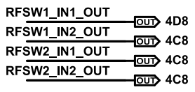
Figure 12. Single Inline Package (SIP) Interface
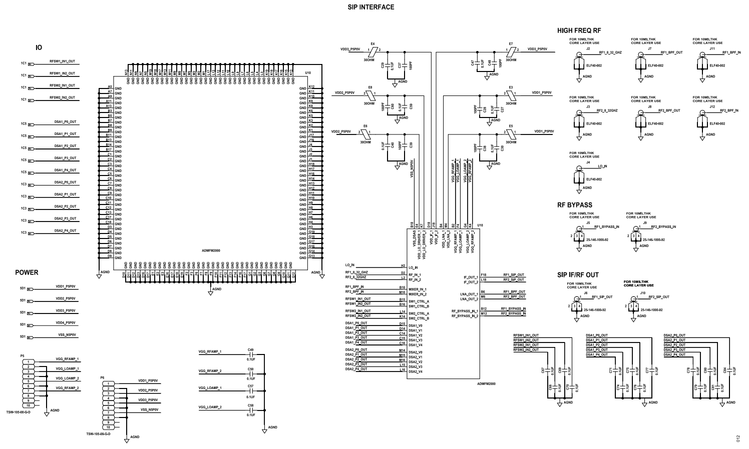
Figure 13. DC Inputs
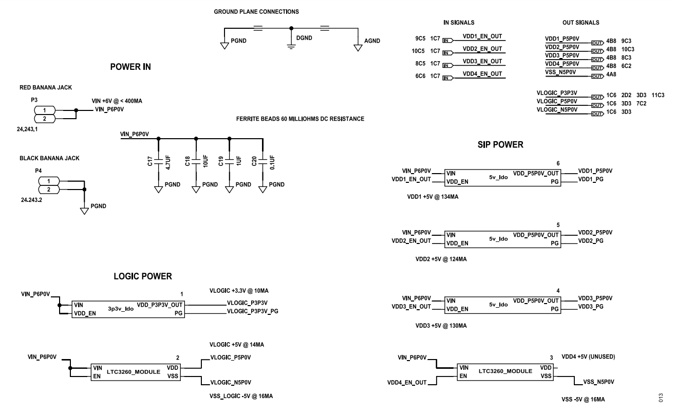
Figure 14. 3.3 V Regulator

Figure 15. Power Regulation
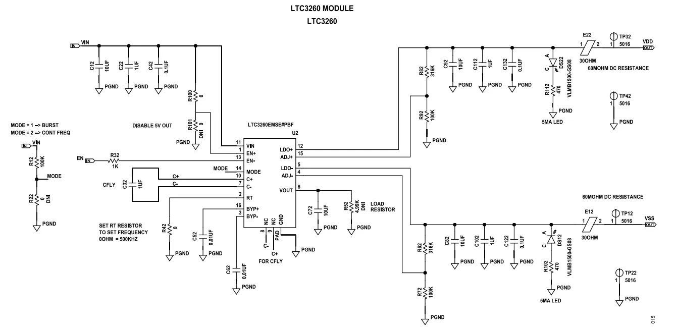

Figure 17. 5 V Regulator
ORDERING INFORMATION
BILL OF MATERIALS
Table 3. Bill of Materials
| Reference Designator | Description | Manufacturer | Part Number |
| C1 to C10, C20, C27, C29 to C31, C34 to C36, C40, C42, C43, C47, C49, C50, C57 to C59, C61, C64 to C71, C74 to C81, C84, C122, C123, C132, C133 | Ceramic capacitors, 0.1 μF, 25 V, 10%, X5R, 0201 | Murata | GRM033R61E104KE14D |
| C19, C21 to C26, C51, C54 to C56, C102, C103, C112, C113 | Ceramic capacitors, 1 μF, 25 V, 10%, X7R, 0805, AEC- Q200 | Murata | GCM21BR71E105KA56L |
| C11 to C16, C18, C41, C44 to C46, C72, C73, C82, C83, C92, C93 | Ceramic capacitors, 10 μF, 25 V, 10%, X7S, 0805 | Murata | GRM21BC71E106KE11L |
| C17 | Ceramic capacitor, 4.7 μF,F, 25 V, 10%, X7R, 1206 | KEMET | C1206C475K3RACTU |
| C28, C37 to C39, C48, C60 | Ceramic capacitors, 100 pF, 50 V, 5%, C0G, 0201 | Murata | GRM0335C1H101JA01D |
| C32, C33 | Ceramic capacitors, 1 μF, 50 V, 10%, X7R, 1206, AEC- Q200 | Murata | GCJ31MR71H105KA12L |
| C52, C53, C62, C63 | Ceramic capacitors, 0.01 μF, 25 V, 10%, X5R, 0201 | Murata | GRM033R61E103KA12D |
| DS11 to DS16, DS22, DS23 | Light emitting diode (LED) chip, ultrabright, 45 mcd, 475 nm, blue | VISHAY | VLMB1500-GS08 |
| E3 to E8, E11 to E16, E22, E23 | Ferrite beads, 30 Ω, 0402, 1LN | Murata Manufacturing | BLM15AX300SN1D |
| J1 | Connector for the SDP controller board | HRS | FX8-120S-SV(21) |
| J5, J6, J9, J10 | Connectors, edge launch jack, 38 GHz | SRI Connector Gage Co. | 25-146-1000-92 |
| J2 to J4, J7, J8, J11, J12 | Connectors, 2.9 mm, end launch, edge-mount jack, 40 GHz | Signal Microwave | ELF40-002 |
| P1, P2 | Connectors, breakout headers connected to the SDP interface | Wurth Elektronik | 610120249121 |
| P3 | Connector, banana jack, red for VCC | Multicomp (SPC) | 24.243.1 |
| P4 | Connector, banana jack, black for GND | Multicomp (SPC) | 24.243.2 |
| P5, P6 | Connectors (CONN), printed circuit board (PCB), header, straight, 10 position | Samtec | TSW-105-08-G-D |
| R1 | Resistor, surface-mount device (SMD), 1 MΩ, 1%, ¼ W, 1206 | IRCTT Electronics | WCR1206-1M0FI |
| R7 to R10, R18, R32, R33, R37 to R40, R49 to R51, R54, R55, R64, R65, R67 to R70, R77 | Resistors, SMD, 1 kΩ, 1%, 1/20 W, 0201 | Panasonic | ERJ-1GNF1001C |
| R42, R43, R100, R1003 | Resistors, SMD, 0 Ω, JUMPER, 1/20 W, 0201 | Panasonic | ERJ-1GN0R00C |
| R44 to R46, R102, R103, R112, R113 | Resistors, SMD, 470 Ω, 5%, 1/10 W, 0402, AEC-Q200 | Panasonic | ERJ-2GEJ471X |
| R11 to R16, R21, R24 to R26, R31, R34 to R36 | Resistors, SMD, 100 kΩ, 1%, 1/20 W, 0201 | Panasonic | ERJ-1GNF1003C |
| R6, R17, R19, R20, R27 to R30, R47, R48, R56 to R61, R66, R71, R74 to R76, R78 to R81, R84 to R91, R94 to R99 | Resistors, SMD, 10 kΩ, 5%, 1/20 W, 0201 | Panasonic | ERJ-1GNJ103C |
| R3, R4 | Resistors, SMD, 100 kΩ, 1%, 1/16 W, 0603 | Multicomp (SPC) | MC 0.063W 0603 1% 100K |
| R41 | Resistor, SMD, 80.6 Ω, 1%, 1/16 W, 0402 | Yageo | RC0402FR-0780R6L |
| R62, R63, R82, R83 | Resistors, SMD, 316 kΩ, 1%, 1/20 W, 0201, AEC-Q200 | Panasonic | ERJ1GNF3163C |
| R72, R73, R92, R93 | Resistors, SMD, 100 kΩ, 5%, 1/10 W, 0402, AEC-Q200 | Panasonic | ERJ-2GEJ104X |
| R22, R23, R101, R1013 | Resistors, SMD, 0 Ω, jumper, 1/20 W, 0201, do not install (DNI) | Panasonic | ERJ-1GN0R00C |
| R2, R5 | Resistors, SMD, 0 Ω, jumper, 1/10 W, 0603, AEC-Q200, DNI | Panasonic | ERJ-3GEY0R00V |
| R52, R53 | Resistors, SMD, 4.99 kΩ, 1% ,1/8 W, 0805, AEC-Q200, DNI | Panasonic | ERJ-6ENF4991V |
| S1 | Digital control select switch, SPDT, where the SPI and general-purpose input and output (GPIO) controls are enabled with the switch on the S1 silkscreen position; otherwise, the optional manual control is effective | C&K | JS102011JCQN |
| S2 | Switch, SPST, four sections, manual enablement of the on-board voltage regulation circuits1 | CTS Electronic Components | 204-4ST |
| S3 | Switch, SPST, four sections, manual control of the mixer/bypass switch internal to ADMFM20001 | CTS Electronic Components | 204-4ST |
| S4, S5 | Switches, SPST, manual DSA controls1 | CTS Electronic Components | 204-5ST |
| TP11 to TP16, TP21 to TP26, TP32, TP33, TP42, TP43 | Test points | Keystone Electronics | 5016 |
| U1 | IC, 32Kb SERIAL EEPROM, storage for information allowing the SDP system to connect to ADMFM2000 | Microchip Technology | 24LC32A/SN |
| U10 | Dual-channel, 0.5 GHz to 32 GHz, microwave downconverter | Analog Devices | ADMFM2000 |
| U11 | 20 V, 300 mA, low noise, CMOS low dropout (LDO) regulator | Analog Devices | ADP7102ACPZ-3.3-R7 |
| U6, U8, U9, U12, U13 | 4 Ω RON, quad SPDT, ±15 V/+12 V/±5 V iCMOS switches | Analog Devices | ADG1434YRUZ |
| U14 to U16 | 20 V, 300 mA, low noise, CMOS low dropout (LDO) regulator | Analog Devices | ADP7102ACPZ-5.0-R7 |
| U2, U3 | Low noise, dual-supply, inverting charge pump | Analog Devices | LTC3260EMSE#PBF |
| U4, U5, U7 | 9.5 Ω RON, ±15 V/+12 V/±5 V iCMOS, serially controlled octal SPST switches | Analog Devices | ADG1414BRUZ |
- Controlling the ADMFM2000 through the GUI is recommended. Manual control is optional. Refer to the Evaluation Board Schematics section and the ADMFM2000 data sheet for the connection details of each manual switch.
![]() ESD Caution
ESD Caution
ESD (electrostatic discharge) sensitive device. Charged devices and circuit boards can discharge without detection. Although this product features patented or proprietary protection circuitry, damage may occur on devices subjected to high energy ESD. Therefore, proper ESD precautions should be taken to avoid performance degradation or loss of functionality.
Legal Terms and Conditions
By using the evaluation board discussed herein (together with any tools, components documentation or support materials, the “Evaluation Board”), you are agreeing to be bound by the terms and conditions set forth below (“Agreement”) unless you have purchased the Evaluation Board, in which case the Analog Devices Standard Terms and Conditions of Sale shall govern. Do not use the Evaluation Board until you have read and agreed to the Agreement. Your use of the Evaluation Board shall signify your acceptance of the Agreement. This Agreement is made by and between you (“Customer”) and Analog Devices, Inc. (“ADI”), with its principal place of business at Subject to the terms and conditions of the Agreement, ADI hereby grants to Customer a free, limited, personal, temporary, non-exclusive, non-sublicensable, non-transferable license to use the Evaluation Board FOR EVALUATION PURPOSES ONLY. Customer understands and agrees that the Evaluation Board is provided for the sole and exclusive purpose referenced above, and agrees not to use the Evaluation Board for any other purpose. Furthermore, the license granted is expressly made subject to the following additional limitations: Customer shall not (i) rent, lease, display, sell, transfer, assign, sublicense, or distribute the Evaluation Board; and (ii) permit any Third Party to access the Evaluation Board. As used herein, the term “Third Party” includes any entity other than ADI, Customer, their employees, affiliates and in-house consultants. The Evaluation Board is NOT sold to Customer; all rights not expressly granted herein, including ownership of the Evaluation Board, are reserved by ADI. CONFIDENTIALITY. This Agreement and the Evaluation Board shall all be considered the confidential and proprietary information of ADI. Customer may not disclose or transfer any portion of the Evaluation Board to any other party for any reason. Upon discontinuation of use of the Evaluation Board or termination of this Agreement, Customer agrees to promptly return the Evaluation Board to ADI. ADDITIONAL RESTRICTIONS. Customer may not disassemble, decompile or reverse engineer chips on the Evaluation Board. Customer shall inform ADI of any occurred damages or any modifications or alterations it makes to the Evaluation Board, including but not limited to soldering or any other activity that affects the material content of the Evaluation Board. Modifications to the Evaluation Board must comply with applicable law, including but not limited to the RoHS Directive. TERMINATION. ADI may terminate this Agreement at any time upon giving written notice to Customer. Customer agrees to return to ADI the Evaluation Board at that time. LIMITATION OF LIABILITY. THE EVALUATION BOARD PROVIDED HEREUNDER IS PROVIDED “AS IS” AND ADI MAKES NO WARRANTIES OR REPRESENTATIONS OF ANY KIND WITH RESPECT TO IT. ADI SPECIFICALLY DISCLAIMS ANY REPRESENTATIONS, ENDORSEMENTS, GUARANTEES, OR WARRANTIES, EXPRESS OR IMPLIED, RELATED TO THE EVALUATION BOARD INCLUDING, BUT NOT LIMITED TO, THE IMPLIED WARRANTY OF MERCHANTABILITY, TITLE, FITNESS FOR A PARTICULAR PURPOSE OR NONINFRINGEMENT OF INTELLECTUAL PROPERTY RIGHTS. IN NO EVENT WILL ADI AND ITS LICENSORS BE LIABLE FOR ANY INCIDENTAL, SPECIAL, INDIRECT, OR CONSEQUENTIAL DAMAGES RESULTING FROM CUSTOMER’S POSSESSION OR USE OF THE EVALUATION BOARD, INCLUDING BUT NOT LIMITED TO LOST PROFITS, DELAY COSTS, LABOR COSTS OR LOSS OF GOODWILL. ADI’S TOTAL LIABILITY FROM ANY AND ALL CAUSES SHALL BE LIMITED TO THE AMOUNT OF ONE HUNDRED US DOLLARS ($100.00). EXPORT. Customer agrees that it will not directly or indirectly export the Evaluation Board to another country, and that it will comply with all applicable United States federal laws and regulations relating to exports. GOVERNING LAW. This Agreement shall be governed by and construed in accordance with the substantive laws of the Commonwealth of Massachusetts (excluding conflict of law rules). Any legal action regarding this Agreement will be heard in the state or federal courts having jurisdiction in Suffolk County, Massachusetts, and Customer hereby submits to the personal jurisdiction and venue of such courts. The United Nations Convention on Contracts for the International Sale of Goods shall not apply to this Agreement and is expressly disclaimed.
©2024 Analog Devices, Inc. All rights reserved. Trademarks and registered trademarks are the property of their respective owners. One Analog Way, Wilmington, MA 01887-2356, U.S.A.
