![]()
ASEK71020
ACS71020 Evaluation Board User Guide
Contents
DESCRIPTION
The Allegro ACS71020 evaluation board is pictured in Figure 1. Refer to Table 1 for symbol names and descriptions of onboard components. Note: Board is pictured without capacitors and resistors attached.
EVALUATION BOARD CONTENTS

- ASEK71020 Evaluation Board
Table 1: Summary of Evaluation Board Components
| Symbol | Description |
| U1 | Location of Allegro ACS71020 |
| U2 | Voltage regulator |
| C1/C2 | 0.1 µF regulator capacitors |
| C3 | 0.1 µF device bypass capacitor |
| R1 | RSENSE resistor voltage step down circuit; application specific |
| R2-R5 | Digital I/O pull-up resistors (used for SPI or I2C communication) |

PINOUT DIAGRAM AND TERMINAL LIST

Pinout Diagram
Table 2: Terminal List
| Number | Name | Description | |
| I2C | SRI | ||
| 1,2, 3, 4 | IP+ | Terminals for current being sensed; fused internally | |
| 5,6, 7,8 | IP- | Terminals for current being sensed; fused internally | |
| 9 | DIO _1/CS | Digital I/O 1 | Chip Select (CS) |
| 10 | DIO_ 0/MOSI | Digital I/O 0 | MOSI |
| 11 | SCL /SCLK | SCL | SCLK |
| 12 | SDA /MISO | SDA | MISO |
| 13 | VCC | Device power supply terminal | |
| 14 | GND | Device Power and Signal ground terminal | |
| 15 | VINN | Negative Input Voltage | |
| 16 | VINP | Positive Input Voltage | |
ACS71020 Recommended Application Circuit
A resistor divider circuit shall be used to step down measured the voltage of the system. The voltage across VINP and VINN shall not exceed 275 mV as stated in the datasheet. This application example steps the voltage down to ±250 mV for expected Vpeak. The standard application schematic is shown in Figure 3. Refer to the ACS71020 device datasheet for more information.

Step-Down Circuit
Figure 4 shows the step-down application circuit in finer detail. The appropriate value for the sense resistor “R” shall be determined by the user as to not exceed 275 mV across VINP and VINN.
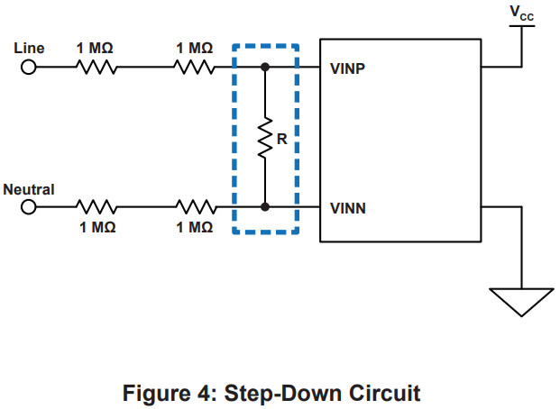
Table 3 shows recommended resistor values for popular application voltages, and assumes the step down circuit in Figure 4.
Table 3: Recommended RSENSE based on VRMS
| VRMS (V) | Vpeak (V) | Range of VIN (V) | R Max(Ω) | RSENSE Recommended (kΩ) |
| 50 | 70.7 | 0.25 | 14194 | 13 |
| 100 | 141.4 | 0.25 | 7085 | 5.6 |
| 110 | 155.54 | 0.25 | 6440 | 5.1 |
| 120 | 169.68 | 0.25 | 5902 | 4.7 |
| 150 | 212.1 | 0.25 | 4720 | 3.9 |
| 220 | 311.08 | 0.25 | 3217 | 2.2 |
| 240 | 339.36 | 0.25 | 2949 | 1.8 |
Revision History
| Number | Date | Description |
| – | 12-Jul-17 | Initial release |
| 1 | 26-Jul-19 | Minor editorial updates |
| 2 | 16-Aug-23 | Minor editorial updates |
Copyright 2023, Allegro MicroSystems.
The information contained in this document does not constitute any representation, warranty, assurance, guaranty, or inducement by Allegro to the customer with respect to the subject matter of this document. The information being provided does not guarantee that a process based on this information will be reliable, or that Allegro has explored all of the possible failure modes. It is the customer’s responsibility to do sufficient qualification testing of the final product to ensure that it is reliable and meets all design requirements.
Copies of this document are considered uncontrolled documents.
For the latest version of this document, visit our website:
www.allegromicro.com
![]()
Allegro MicroSystems
955 Perimeter Road
Manchester, NH 03103-3353 U.S.A.
www.allegromicro.com