PiezoDrive PX200 Power Amplifier Owner’s Manual

Contents
Introduction
The PX200 is a low-noise high-current linear amplifier for driving piezoelectric actuators and other loads. The output voltage range can be unipolar, bipolar, or asymmetric from 50V to 200V. Refer to the specifications table for the available output voltage ranges. Two amplifiers can be connected in bridge-mode to provide up to +/-200V or +400V. The PX200 has a high output current up to 13 Amps peak and is well suited to precision applications that require high power and frequency. The PX200 can drive any load impedance including unlimited capacitive loads such as stack actuators; standard piezoelectric actuators; two wire benders; and three-wire piezoelectric benders requiring a bias voltage. Bias voltages can be generated using two auxiliary outputs linked to the power supply voltages.
A range of front panel controls provide maximum application flexibility, these include input signal inversion, variable gain, DC offset, and variable voltage limits. A 9-pin DSUB connector on the front panel includes signals for the input, voltage monitor, current monitor, shutdown monitor, and shutdown command. A four-digit LCD screen also displays the DC voltage. The output connectors include BNC, LEMO 00, LEMO 0B.302, and plug-in screw terminals. The PX200 is suited to a wide range of applications including electro-optics, ultrasonics, vibration control, nanopositioning systems, and piezoelectric motors.
| Compatible Actuators | |
| Stack Actuators | Up to +200V |
| Plates and Tubes | +/-100V or +200V |
| Two Wire Benders | +/-100V or +200V |
| Three Wire Benders | Up to +200V with +200V bias, or +/-100V with +/-100V bias |
 Warnings / Notes
This device produces hazardous potentials and requires suitably qualified personnel with an observer trained in first-aid training. Do not operate the device when there are exposed conductors.
Output Voltage Ranges
The output voltage range is specified when ordering. The standard voltage ranges and associated current limits are listed below. Since the PX200 has front panel controls for reducing the positive and negative output voltage range, choose a range equal to or slightly greater than required.
| NegativeVoltage (Volts) | PositiveVoltage (Volts) | RMSCurrent (Amps) | PeakCurrent (Amps) | PulseCurrent [1] | Gain [2] | Var [3] | Order Code |
| 0 | 200 | 1.6 | 3 | 9 | 20 | A | PX200-P200 |
| 0 | 150 | 2.1 | 4 | 10 | 15 | A | PX200-P150 |
| -50 | 150 | 1.6 | 3 | 9 | 15 | A | PX200-N50-P150 |
| -50 | 100 | 2.1 | 4 | 10 | 10 | A | PX200-N50-P100 |
| -100 | 100 | 1.6 | 3 | 9 | 10 | A | PX200-N100-P100 |
| -100 | 50 | 2.1 | 4 | 10 | 10 | A | PX200-N100-P50 |
| -100 | 0 | 3.1 | 6 | 13 | 10 | A | PX200-N100 |
| -150 | 0 | 2.1 | 4 | 10 | 15 | A | PX200-N150 |
| -200 | 0 | 1.6 | 3 | 9 | 20 | A | PX200-N200 |
| 0 | 175 | 1.8 | 3 | 10 | 20 | B | PX200-P175 |
| -25 | 150 | 1.8 | 3 | 10 | 15 | B | PX200-N25-P150 |
| -25 | 100 | 2.7 | 4 | 10 | 10 | B | PX200-N25-P100 |
| -75 | 100 | 1.8 | 3 | 10 | 10 | B | PX200-N75-P100 |
| -75 | 50 | 2.7 | 4 | 10 | 10 | B | PX200-N75-P50 |
| 0 | 125 | 2.7 | 4 | 10 | 15 | D | PX200-P125 |
| -25 | 125 | 2.1 | 4 | 10 | 15 | D | PX200-N25-P125 |
| -75 | 75 | 2.1 | 4 | 10 | 10 | D | PX200-N75-P75 |
| 0 | 100 | 3.1 | 6 | 13 | 10 | E | PX200-P100 |
| 0 | 75 | 4.1 | 6 | 13 | 10 | E | PX200-P75 |
| 0 | 50 | 5.3 | 9 | 13 | 10 | E | PX200-P50 |
| 0 | 25 | 5.3 | 9 | 13 | 10 | E | PX200-P25 |
| -25 | 75 | 3.1 | 6 | 13 | 10 | E | PX200-N25-P75 |
| -25 | 50 | 4.1 | 6 | 13 | 10 | E | PX200-N25-P50 |
| -25 | 25 | 5.3 | 9 | 13 | 10 | E | PX200-N25-P25 |
| -50 | 50 | 3.1 | 6 | 13 | 10 | E | PX200-N50-P50 |
| -50 | 25 | 4.1 | 6 | 13 | 10 | E | PX200-N50-P25 |
| -50 | 0 | 5.3 | 9 | 13 | 10 | E | PX200-N50 |
| -75 | 0 | 4.1 | 6 | 13 | 10 | E | PX200-N75 |
| -100 | 0 | 3.1 | 6 | 13 | 10 | E | PX200-N100 |
Notes:
- Refer to Section 6 for details on the pulse current limit
- The gain can be increased by up to another factor of 10 using the front panel control
- The variant is the hardware version required for the chosen configuration
Output Current
The peak and RMS output current is listed in Table 1. The RMS current limit determines the maximum frequency that is achievable with a capacitive load. A calculator for the maximum operating frequency is provided in Section 5. During short-circuit the output current is limited to the rated maximum. The peak current can be drawn for up to five milliseconds before the output is disabled for three seconds. The average current limit has a time-constant of ten milliseconds and is reset 50 milliseconds after a previous current pulse. This behaviour is described in Section 13.
Higher peak currents are achievable with the PULSE option, which is described in Section 6.
Power Bandwidth
 Launch Online Power Bandwidth Calculator
The online power bandwidth calculator estimates the highest achievable frequency with a capacitive load impedance. The calculator considers the current limit, slew-rate, output impedance, and smallsignal bandwidth. With a capacitive load, the maximum operating frequency due to the RMS current limit is
???? = ????√2/????? ,
where ???? is the current limit, ??? is the peak-to-peak output voltage, ? is the load capacitance. The above equation is also true for any periodic waveform, including triangle waves and square waves. The ‘power bandwidth’ is the maximum frequency at full output voltage. When the amplifier output is open-circuit, the power bandwidth is limited by the slew-rate; however, with a capacitive load, the maximum frequency is limited by the RMS current and load capacitance. The power bandwidth for a range of capacitive loads is listed below
| Load | 50 Vp-p | 75 Vp-p | 100 Vp-p | 125 Vp-p | 150 Vp-p | 175 Vp-p | 200 Vp-p |
| 10 nF | 222930* | 148620* | 111465* | 89172* | 74310* | 63694* | 55732* |
| 30 nF | 222930* | 148620* | 111465* | 89172* | 74310* | 63694* | 55732* |
| 100 nF | 222930* | 148620* | 111465* | 89172* | 62000 | 45714 | 35000 |
| 300 nF | 160000 | 82667 | 46667 | 32000 | 20667 | 15238 | 11667 |
| 1 uF | 48000 | 24800 | 14000 | 9600 | 6200 | 4571 | 3500 |
| 3 uF | 16000 | 8267 | 4667 | 3200 | 2067 | 1524 | 1167 |
| 10 uF | 4800 | 2480 | 1400 | 960 | 620 | 457 | 350 |
| 30 uF | 1600 | 827 | 467 | 320 | 207 | 152 | 117 |
In the above table, the frequencies limited by slew-rate are marked with an asterisk. The slew-rate is
approximately 35 V/uS which implies a maximum frequency of
???? = 35 × 106/???p
Pulse Current Option
The PULSE current option provides a higher peak current for approximately 150 us instead of the standard 5 ms. This option is useful in specialty applications that require fast, small changes in the output voltage with large capacitive loads. The achievable step change in voltage is,
Δ? = ??? ??????/?????
where, Δ? is the step change in Volts, ??? is the pulse current limit of the amplifier, and ?????? is the maximum pulse time of the amplifier, listed below. With large capacitive loads, it may not be possible to step between the minimum and maximum output voltage. The maximum capacitance where a full range step can by sustained is approximately,
???? = ??? ??????/Δ?
The PULSE option provides approximately three times higher peak-current, but less than one-tenth of the permissible overload time compared to the standard option. Therefore, the PULSE option provides approximately one-third of the Δ? and ???? compared to the standard version and should only be selected for applications where the higher peak current is worth the reduction in permissible overload time. With waveforms that do not require step changes in voltage, such as sinusoidal and triangular signals, the standard configuration is preferrable. At frequencies below 1kHz, the PULSE option will result in lower-than-expected power bandwidth as the signal rise time will exceed 500us and may trigger the overcurrent protection. The pulse current limits for each configuration are listed in Table 1 and summarized in Table 3. The output voltage span is the peak-to-peak output voltage range, e.g. the voltage span for the -50V to +150V range is 200V.
| Output Voltage Span | Pulse Current | Pulse Time | Cmax (full step) |
| 200 Vp-p | 9 A | 150 us | 6.7 uF |
| 175 Vp-p | 10 A | 155 us | 8.8 uF |
| 150 Vp-p | 10 A | 180 us | 12 uF |
| 125 Vp-p | 10 A | 236 us | 18 uF |
| 100 Vp-p | 13 A | 211 us | 27 uF |
| 75 Vp-p | 13 A | 286 us | 49 uF |
| 50 Vp-p | 13 A | 378 us | 98 uF |
| 25 Vp-p | 13 A | 378 us | 196 uF |
The maximum pulse duration versus peak current is described in Figure 1. The pulse current option can be ordered by appending the order code with “-PULSE”, e.g. “PX200-P200-PULSE”.

Specifications
The voltage, current, and gain specifications are listed in Table 1. Other specifications that are common to all configurations are listed below.
| Specification | Value |
| Slew Rate | 35 V/us |
| Signal Bandwidth | 390 kHz |
| Max Power | 140 W Dissipation |
| Load | Any |
| Noise | 150 uV RMS (10uF Load, 0.03 Hz to 1 MHz) |
| Protection | Continuous short-circuit, thermal |
| Voltage Monitor | 1/20 V/V |
| Current Monitor | 1.5 V/A if peak current is 6 Amps or less0.5 V/A if peak current is greater than 6 Amps |
| Input Impedance | 48.7 kOhms |
| Output Impedance | 1.5 Ohms |
| Output Connectors | LEMO 0B, LEMO 00, Screw Terminals, BNC |
| Power Supply | 90 Vac to 250 Vac |
| Environment | 0-40 C (32-104 F) Non-condensing humidity |
| Dimensions | 212 x 304.8 x 88 mm (8.35 x 12 x 3.46 in) |
| Weight | 2 kg (4.4 lb) |
Small Signal Bandwidth
The small-signal frequency response and -3 dB bandwidth is described in Figure 2 and Table 4.
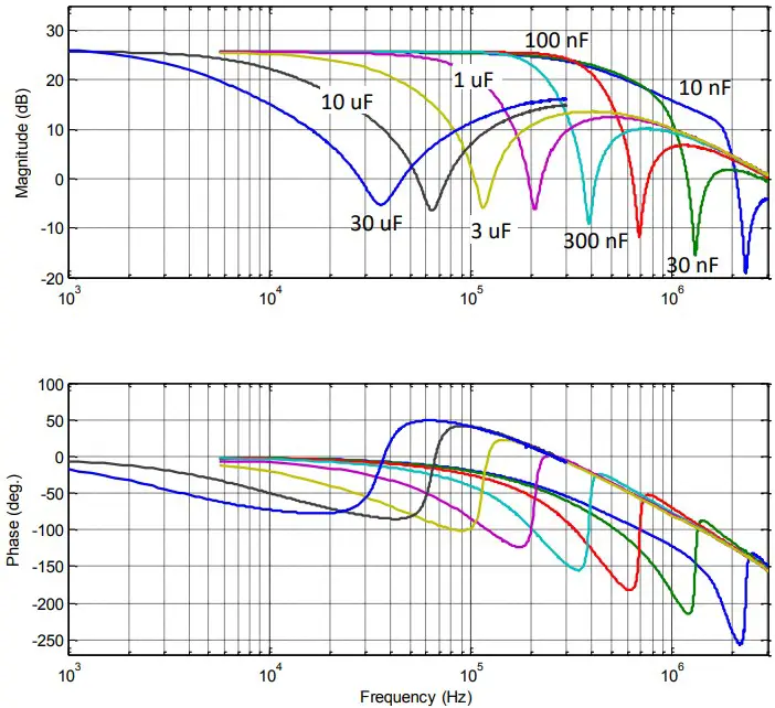
| Load Capacitance | Bandwidth |
| 10 nF | 393 kHz |
| 30 nF | 431 kHz |
| 100 nF | 367 kHz |
| 300 nF | 208 kHz |
| 1 uF | 88 kHz |
| 3 uF | 30 kHz |
| 10 uF | 9.3 kHz |
| 30 uF | 3.7 kHz |
| 110 uF | 1.3 kHz |
Noise
The output voltage noise contains a low frequency component (0.03 Hz to 20 Hz) that is independent of the load capacitance; and a high frequency (20 Hz to 1 MHz) component that is approximately inversely proportional to the load capacitance. The noise is measured with an SR560 low-noise amplifier (Gain = 1000), oscilloscope, and Agilent 34461A Voltmeter. The low-frequency noise is plotted in Figure 3. The RMS value is 120 uV with a peak-to-peak voltage of 600 uV.

The high frequency noise (20 Hz to 1 MHz) is listed in the table below versus load capacitance. The total RMS noise from 0.03 Hz to 1 MHz is found by summing the RMS values, that is ? = √???2 + ???2.
For a load capacitance of less than 1 uF, the noise is primarily broadband thermal noise; however, for a capacitance of greater than 1 uF, the noise is primarily due to low-frequency noise.
| Load | Bandwidth | HF Noise RMS | Total Noise RMS |
| 10 nF | 393 kHz | 530 uV | 543 uV |
| 30 nF | 431 kHz | 586 uV | 598 uV |
| 100 nF | 367 kHz | 689 uV | 699 uV |
| 300 nF | 208 kHz | 452 uV | 468 uV |
| 1 uF | 88 kHz | 261 uV | 287 uV |
| 3 uF | 30 kHz | 106 uV | 160 uV |
| 10 uF | 9.3 kHz | 56 uV | 132 uV |
| 30 uF | 3.7 kHz | 52 uV | 131 uV |
| 100 uF | 1.3 kHz | 47 uV | 129 uV |
Front Panel
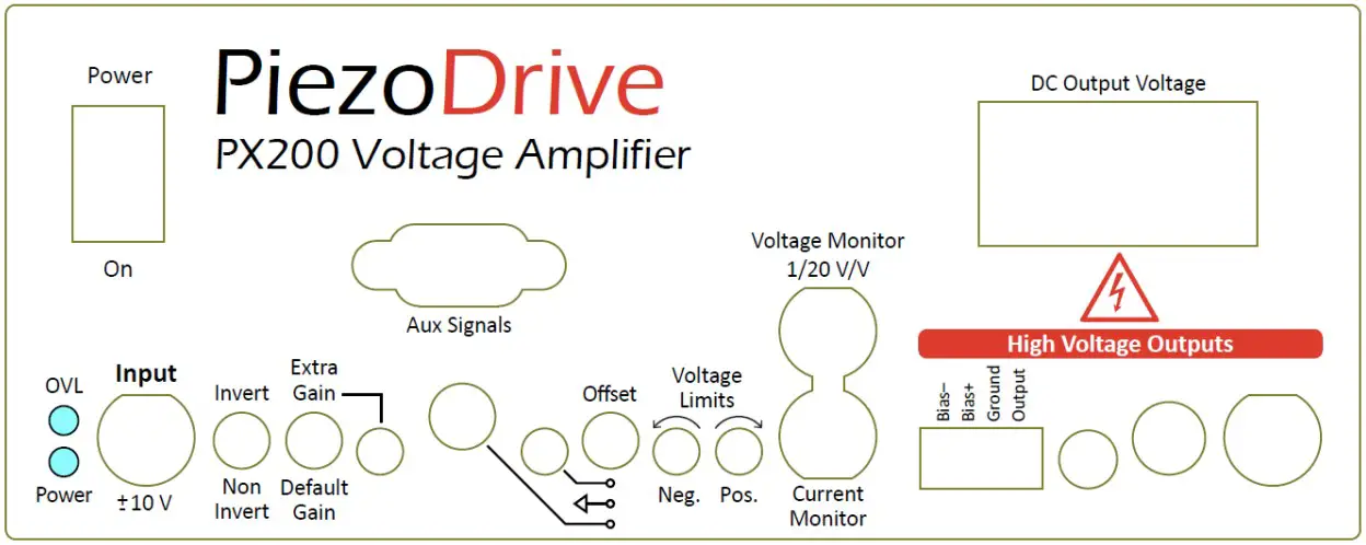
| Control | Type | Function |
| Power | Power On/Off | |
| Overload LED | RED when the amplifier is disabled or in an overload state | |
| Power LED | GREEN when the power is on | |
| Input | Input | Input signal (±10V max, protected up to +/-20V) |
| Invert switch | Multiplies the input signal by -1 in the upward position | |
| Gain switch | Adds additional gain to the input signal when in the upward position | |
| Gain pot | Clockwise rotation increases the additional gain (up to a factor of 10) | |
| Offset knob | Single turn potentiometer for DC offset | |
| Offset pot | Multiple turn potentiometer for DC offset | |
| Offset switch | Selects between the offset sources, or zero in the middle position | |
| Voltage Limits | Limits the maximum negative and positive output voltage | |
| Voltage Monitor | Output | The measured output voltage, scaled by 1/20 |
| Current Monitor | Output | The measured output current, 1.5 V/A or 0.5 V/A (See Section 0) |
| Bias- | Output | DC Bias connected to the negative high-voltage power supply rail |
| Bias+ | Output | DC Bias connected to the positive high-voltage power supply rail |
| Ground | Output | Ground, connect to the load negative terminal |
| Output | Output | Amplifier output, connect to the load positive terminal |
| LEMO 00 Output | Output | EPL.00.250 connector, suits LEMO FFA.00.250 cable plug |
| LEMO 0B Output | Output | FGG.0B.302 connector, suits LEMO FGG.0B.302 cable plug |
| BNC Output | Output | Suits male BNC cable plug |
| DC Output Volt. | Display showing average output voltage |
The screw terminals or LEMO 0B.302 connector are recommended for applications requiring more than 1 Amp RMS output current. Preassembled LEMO cable assemblies (e.g. PD-0B302-W-120) are available from www.PiezoDrive.com
The auxiliary signals connector is a 9-way DSUB receptacle which suits any 9-way male DSUB plug. The signals and pin layout are shown in Figure 4 and Table 6.
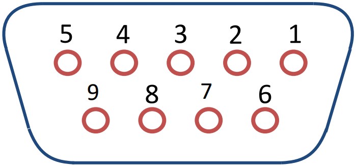
| Signal | Pin | Function |
| Input+ | 1 | Input signal |
| Input- | 2 | Ground for input signal |
| Voltage Monitor | 3 | Voltage monitor |
| Current Monitor | 4 | Current monitor |
| Ground | 5 | Ground |
| Shutdown | 6 | +2V to +20V disables the amplifier |
| Shutdown Monitor | 7 | +5V when the amplifier is shutdown |
| NC | 8, 9 | Not connected |
Signal Path

Voltage Limits
The output voltage range can be restricted to an arbitrary positive and negative value using two potentiometers on the front panel. To set the voltage limit:
- Remove loads connected to the outputs
- Apply a 100-Hz sine wave to the input of channel 1 with an amplitude that covers the full range of the amplifier. For example, with a 0V to +200V model, apply a 0V to +10V input.
- Measure the output voltage of channel 1 with an oscilloscope and confirm the full voltage range is achieved. If there is any clipping of the sine wave, the voltage limits may have already been set, and may need resetting by winding the potentiometers in the direction of the arrows.
- To limit either the negative or the positive voltage, turn the potentiometer in the opposite direction to the arrow, until the voltage is limited to the desired level.
Overload and Shutdown
The amplifier is protected against short-circuit, over-current, and excessive temperature. During these conditions, the front panel overload indicator will illuminate, and the Shutdown Monitor signal is +5V. During an overload or shutdown state, the output is partially disabled and may float at approximately 50% of the voltage range. When the amplifier is switched on, the overload protection circuit is engaged by default and clears after three seconds.The amplifier can be shut down by an external source by applying a voltage of between +2V and +24V to the Shutdown input. The impedance of the shutdown input is approximately 5 kΩ.
Bias Outputs and Piezo Benders
The bias outputs are labelled HV+ and HV- on the front-panel screw terminals. The output voltages are fixed at the maximum output voltages of the amplifier and are not affected by the voltage limit potentiometers. For example, a PX200-N100-P100 (with a +/-100V output range) will output +100V and -100V on HV+ and HV- respectively. For amplifier configurations where the HV- output is zero (e.g. PX200-P200), it is preferable to use ground rather than the HV- output.
The bias outputs provide a small DC output current of approximately 30mA; however, they can source or sink large AC currents, which is ideal for driving piezoelectric actuators. Bender actuators can be driven with a single or dual bias voltage.
The most common bender actuators are parallel-poled and driven using the ‘biased unipolar’ or ‘three-wire’ configuration [1], as shown in Figure 6.

A zero volt input results in +150V across the top piezo layer and maximum upward deflection. A 7.5V input results in +150V across the bottom piezo layer and maximum downward deflection. The deflection ? can be represented by
? = ??? − 7.5/2/7.5
???
where ??? is the peak-to-peak displacement of the bender.
To reduce the maximum DC voltage, a negative bias voltage can be used, as shown in Figure 7.

In Figure 7, the deflection is
? = ???/10 ???
where ??? is the peak-to-peak displacement of the bender.
References
- A New Electrical Configuration for Improving the Range of Piezoelectric Bimorph Benders; S. A. Rios, A. J. Fleming; Sensors and Actuators A: Physical, 2015.
Bridged Mode
In bridged mode, the load is connected between the outputs of two amplifiers, which doubles the output voltage span and power. Grounded loads cannot be driven using bridged mode. Care should be taken not to connect the negative side to ground accidentally, for example, by using a grounded oscilloscope probe.Figure 8 shows how two amplifiers are connected to achieve +/-200V across a load. A +/-10V signal is applied to both amplifiers, and the bottom amplifier is configured in inverting mode. The total voltage across the load is +/-200V and the effective gain is twice the gain of a single amplifier. Common bridged-mode configurations are listed in Table 7. The current limits in bridge mode are identical to normal operation. The power bandwidth calculator can also be used for predicting bridge-mode performance by entering the total voltage across the load. For the example in Figure 8, the total peak-to-peak output voltage is 400V. When entering this value to the calculator, an error will be shown since 400V is greater than the voltage span of a single amplifier; however, the calculator output is remains valid.
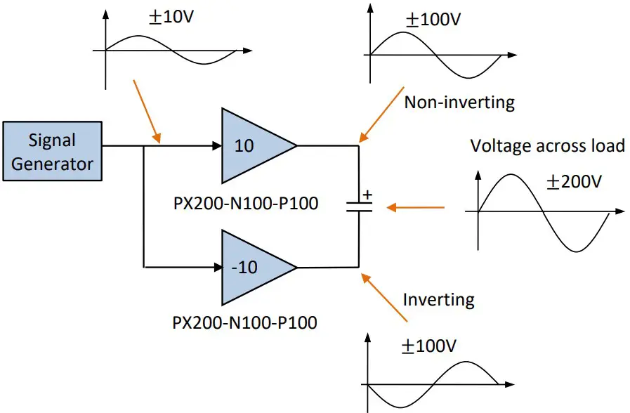
| Load Voltage | RMS Current | Non-Inverting Amp | Inverting Amp |
| ±200V | 1.5 A | PX200-N100-P100 | PX200-N100-P100 |
| ±100V | 3.1 A | PX200-N50-P50 | PX200-N50-P50 |
| 0V to 200V | 3.1 A | PX200-P100 | PX200-N100 |
| 0V to 300V | 2.1 A | PX200-P150 | PX200-N150 |
| 0V to 400V | 1.5 A | PX200-P200 | PX200-N200 |
Rack Mounting
The PX200 can be installed in a 19-inch x 2U rack space using the single unit rack kit (order code: SingleRackKit-2U). Two amplifiers can also be installed in a side-by-side configuration using the double unit rack kit (order code: DoubleRackKit-2U). The double rack kit is assembled in the factory and includes coupling screws for the enclosure, the same handles as the single rack kit, and

Delivery Contents
- PX200 amplifier with plug-in screw terminal installed
- IEC C13 power cable, suited to the shipping destination
Warranty
PiezoDrive amplifiers are guaranteed for 12 months from the date of delivery. The warranty does not cover damage due to misuse.