Auxiliary Power Supply for Industrial and Solar
Applications Using 1.7 kV SiC MOSFET
Contents
Introduction
This document describes the design and performance of a 63W auxiliary power supply with wide input voltage for industrial and solar applications using 1.7 kV Silicon Carbide (SiC) MOSFETs. The evaluation board is designed to evaluate the performance of MSC750SMA170B for ease of use.
This document is for the users of MSC750SMA170B who want to create low-cost and high-performance off-line Switch Mode Power Supply (SMPS) for auxiliary power supply. This document provides the design details, including device selection, control parameter determination, and transformer and hardware designs.
Auxiliary power supply is an essential part of a power converter that converts the electric power from High Voltage (HV) DC bus to a Low Voltage (LV) source for powering control circuits, sensing circuits, cooling fans, and so on. A low power (<100W) power converter with galvanic isolation is one of the most important components in industrial and Photovoltaic (PV) applications. Due to DC link voltage variation, many of these auxiliary power supplies must operate from a wide input voltage range, typically ranging from 250V to 1000V. To ensure the overall reliability of the power converter system, this converter must have a simple topology and a low component count.
Due to its simple structure, low component count, and low cost, the single switch flyback topology is a popular choice for such low power DC-DC converters. However, due to the high peak voltage seen on the power switching device, using silicon MOSFETs in the auxiliary power supply applications presents many challenges.
For example, at the highest input voltage of 1 kV, the peak voltage on the switching device can easily exceed 1.2 kV due to secondary side reflected voltage and voltage across transformer leakage inductance, forcing the user to use 1.5 kV–2 kV devices.
The options for the HV silicon MOSFETs are limited, and the specific on-state resistance is much higher than for LV MOSFETs, reducing the converter efficiency and complicating the cooling design. Furthermore, due to limited resources, the cost of the HV silicon MOSFETs is significantly higher. To utilize the lower rated voltage silicon MOSFETs, two-switch flyback or other topologies can be used, but the design complexity and component count increase significantly, reducing reliability and increasing design cost.
The following figure shows the topology of a single switch flyback converter with a 1.7 kV SiC MOSFET for the auxiliary power supply applications.
Figure 1. Single Switch Flyback Converter for Auxiliary Power Supply Applications
1.7 kV SiC MOSFET is an excellent choice for using a single switch flyback topology in an auxiliary power supply application that requires a wide input voltage range. The 1.7 kV breakdown voltage provides sufficient voltage margin for the 1 kV input voltage. The specific on-resistance of 1.7 kV SiC MOSFET is much lower than that of HV silicon MOSFET, allowing for a smaller die size and lower on-resistance in the same package. The smaller die size also significantly reduces switching loss. This option allows to increase the switching frequency of the auxiliary power supply in order to reduce transformer size and weight.
Features
The evaluation board has the following key hardware features:
- Single Switch Flyback Topology
- 250V–1000V Wide Input Voltage
- +24V/2A and +15V/1A Dual Outputs, and Total 63W Output Power
- High-Power Conversion Efficiency Over Wide Power Range
- Current-Mode Pulse-Width Modulation (PWM) Controller-Based Closed Loop Control
Applications
The evaluation board has the following applications:
- ndustrial motor drives Solar inverters
- Uninterruptible power supplies
- General purpose inverters
- Cascaded H-bridge converters
- Modular multilevel converters
Electrical Specification
The following table lists the electrical specification of the evaluation board.
Table 1-1. Electrical Specification—Evaluation Board
| Symbol | Parameter | Ratings | Unit |
| Vin min | Minimum input voltage | 250 | V |
| Vin max | Maximum input voltage | 1000 | |
| Vout1 | Output voltage 1 | 24 | |
| lout_maxl | Maximum output current 1 | 2 A | |
| Vout2 | Output voltage 2 | 15 V | |
| lout_max2 | Maximum output current 2 | 1 A | |
| Pout max | Maximum output power | 63 | |
| fs | Switching frequency | 45 kHz | |
| Efficiency at >25% load | >80 | 0/0 | |
| Eff max | Peak efficiency | 89 | |
Evaluation Board
This chapter describes the evaluation board hardware, schematics, circuit, and Printed Circuit Board (PCB) layout.
2.1 Evaluation Board Hardware
The main components of the evaluation board include input and output power connectors, input and output capacitors, SiC MOSFET, isolation transformer, output rectifier, driver IC, and analog closed-loop circuits.
The following figure shows the picture of the evaluation board hardware.
Figure 2-1. Evaluation Board Hardware2.2 Schematic
The following components are included in the main power stage circuit:
- A DC input fuse and a Metal Oxide Varistor (MOV) (optional)
- An input capacitor
- A loss reduction startup circuit
- A Resistor Capacitor Diode (RCD) snubber circuit An isolation transformer
- SiC MOSFET A gate driving circuit
- An output rectification circuit
- An isolated output voltage feedback circuit
- An analog control circuit
The control circuit is based on a fixed frequency, high performance, and current-mode PWM controller Integrated Circuit (IC) MIC38C44. The following section describes the detailed design and parameter selection method. To download the actual design files (schematic and gerber files), go to microchip.com/sic.
The following figure shows the schematic of the evaluation board.
Note: The resistance units denoted by k, M, and R in the following figure are kΩ, MΩ, and Ω respectively.
Figure 2-2. Schematic of the Evaluation Board2.3 Circuit Description
The design of a SiC-based single switch flyback converter can be similar to the traditional design of a flyback converter using MIC38C4x controllers. However, some special considerations are discussed in the following sections.
2.3.1 Primary Side SiC Switching Device Selection
For a 1 kV maximum input voltage and the refected voltages at the transformer from the secondary side 24V output voltage, the peak voltage on the primary side switching device can exceed 1.2 kV; thus, 1.7 kV SiC MOSFETs are are selected. The Root Mean Square (RMS) current through the primary side switching device is very low for the rated 63W power, so 750 mΩ SiC MOSFET is more than enough for such applications, while the smaller die size of the 750 mΩ SiC MOSFET can also help to reduce switching loss. Because the peak current through the device is also relatively small, the 3L-TO247 package was chosen for better thermal performance, allowing natural convection cooling to eliminate the need for a fan. Therefore, a 1.7 kV, 750 mΩ SiC MOSFET in an industry standard3L-TO247 package from Microchip (part number MSC750SMA170B) is selected as the primary side switching power device.
2.3.2 Gate Driving Voltage and Gate Resistance Selection
The ultra low gate capacitance of the 1.7 kV, 750 mΩ SiC MOSFET enables direct driving from the controller IC, eliminating the need for an additional gate driver. It is recommended that the gate driving voltage for MSC750SMA170B be +20V/-5V. However, as shown in the following figure, the device works well at +18V with only a slight increase in on-state resistance; even at +15V, the on-state resistance increase is less than 25% at higher junction temperatures. The conduction loss in this application is very low due to the low RMS current through the primary side switch.
Figure 2-3. Normalized On-State Resistance (RDSon) under Different Gate VoltagesFurthermore, because MSC750SMA170B is a normally off device, a negative voltage is not required to keep the device off in a steady state; the recommended negative voltage is to avoid false turn on, which can cause shoot through failure in a half-bridge circuit. There is no risk of shoot through failure in a single switch flyback topology. Therefore, the negative off voltage is not required.
Meanwhile, the controller IC MIC38C44 has an absolute maximum supply voltage of +20V, with special precautions required for operations at ≥ 18V. To ensure the controller IC safe operation, the driving voltage of the SiC MOSFET is set to +17V/0V.
The selection of suitable gate resistance is determined by optimizing switching losses, Electromagnetic Interference (EMI) noise emission, and driving IC capability. A lower gate resistance
increases power MOSFET switching speed and reduces switching loss, while a higher gate resistance reduces converter EMI noise emission. A turn on resistance of 10Ω is selected based on the internal gate resistance of the SiC MOSFET, the peak output current capability, and the output impedance of the PWM controller.
The Undervoltage Lockout (UVLO) of the controller MIC38C44 is relatively low when compared to the optimal gate voltage of the SiC MOSFETs. During the startup process, the controller begins to operate once the supply voltage exceeds the UVLO threshold. When the gate voltage is low, the SiC MOSFET may operate in linear mode, and the maximum current through the device may be less than the current required if the load is heavy. The UVLO can be bypassed, and the threshold voltage can be set through an external circuit. For more information on detailed implementation, contact Microchip technical support.
2.3.3 Control Power Supply and Active Startup
In steady-state operation, the control voltage is generated from the auxiliary winding of the transformer through an 18V zener diode and an NPN transistor. During the startup process, the control voltage is drawn directly from the DC bus. To reduce converter loss and protect the controller from the high DC link voltage, a HV N-channel MOSFET (part number CS3N150AHR) with a high resistance branch is designed for control voltage during startup. Once the voltage on the auxiliary winding of the transformer is built up, the circuit cuts the connection to the HV DC bus to reduce power loss.
It is critical to optimize the gate loop layout design after determining the gate driving parameters. To reduce gate ringing and avoid high peak gate voltage, the key consideration is to reduce gate loop inductance and avoid near-field coupling.
2.3.4 Switching Frequency
The switching frequency of the power converter is one of the most important design parameters because it influences switching losses, transformer losses, overall converter size/weight, and converter level EMI. SiC MOSFETs have low switching loss energy and ultra-low gate charge when compared to Silicon (Si) switches, allowing for higher switching frequency and a more compact transformer design with lower power loss. For this evaluation board, a switching frequency of fs = 45 kHz is selected considering the overall optimization of the converter loss.
2.3.5 Output Voltage Regulation
This demonstration hardware is designed for industrial and solar applications and has two output voltages: 24V/2A for fan loads and 15V/1A for main converter level control circuits. The 24V/2A output is directly regulated by feeding the output voltage back to the controller through an analog compensation network and an opto isolator. The 15V/1A output has an optional second stage power conversion based on the fixed frequency PWM/PFM synchronous buck regulator (MCP16311). If a high precision 15V output is required, the secondary winding of the transformer outputs 18V and feeds it into the buck regulator, which converts it to a precision 15V output. The buck regulator can also be bypassed for cost reduction. In this configuration, the transformer secondary winding
is redesigned for 15V output to comply with the 24V regulation; this transformer design is also available.
2.3.6 Transformer Design
The transformer is the key passive component in the circuit for providing correct output voltages and galvanic isolation. The transformer power loss and temperature rise are determined by the core material and winding wire selection. The leakage inductance, which is determined directly by the winding structure, influences the voltage ringing and peak voltage on the power MOSFET, as well as the RCD clamping circuit design. The isolation capacitance effects the Common Mode (CM) noise emission of the system.
The following table lists the transformer key parameters.
Table 2-1. Transformer Design Specification
| Parameter | Specification |
| Core material | PQ3528 |
| Turns ratio (Np-Ns1-Ns2-Na, Pri:Sec1:Sec2:Aux) | 60:7:5:5 |
| Primary side inductance (LP) | 3.5 mH |
| Isolation rating (pri-sec) | 3000 VAC, 3s, 2.0 mA |
| Isolation resistance (Np-Ns) | 100 MΩ |
| Working temperature | −25 °C–125 °C |
2.3.7 RCD Clamping
To avoid excessive voltage on the primary side switching devices, the flyback topology requires an RCD clamping circuit to absorb the energy in the transformer leakage inductance. When the device drain source voltage is higher than the input plus reflected output voltage, the RCD snubber circuit absorbs the energy from the leakage inductance resonance by forward biasing the diode. The voltage can be assumed constant during one switching period if the snubber capacitance is large enough. To absorb the energy from the transformer leakage inductance, two high power 2W resistors are connected in parallel with one HV 630V/3.9 nF film capacitor.
2.3.7.1 Closed Loop Control Parameter
Closed loop control is used to eliminate steady-state error and reduce the sensitivity of system parametric change. The gain and phase margin of the converter are optimized over a specific frequency range to reduce the influence of small signal load disturbances and improve system load dynamic performance. The closed loop control has minimal influence on the steady state performance. Because the drive IC is configured as a peak current mode PWM controller, an external voltage feedback loop is required to stabilize the converter.
The compensation loop is a typical dual loop design with TL431, the phototransistor optocoupler FOD817A, and the error amplifier inside the controller IC. A detailed RC value calculation for the voltage compensation loop design is not included in this user guide because the purpose of this evaluation board is to demonstrate the power stage performance. For more details, contact the Microchip support team.
2.4 PCB Layout
To reduce system costs, a two-layer PCB configuration is selected. The power loop on the primary side and the gate loop on the secondary side are both minimized for the improved device switching performance and the overall converter performance.
The following figures show the PCB layout design of the demo hardware.
Figure 2-4. PCB Layout DesignFigure 2-5. PCB Layout Design—Top Layer Copper and Top Side Component Placement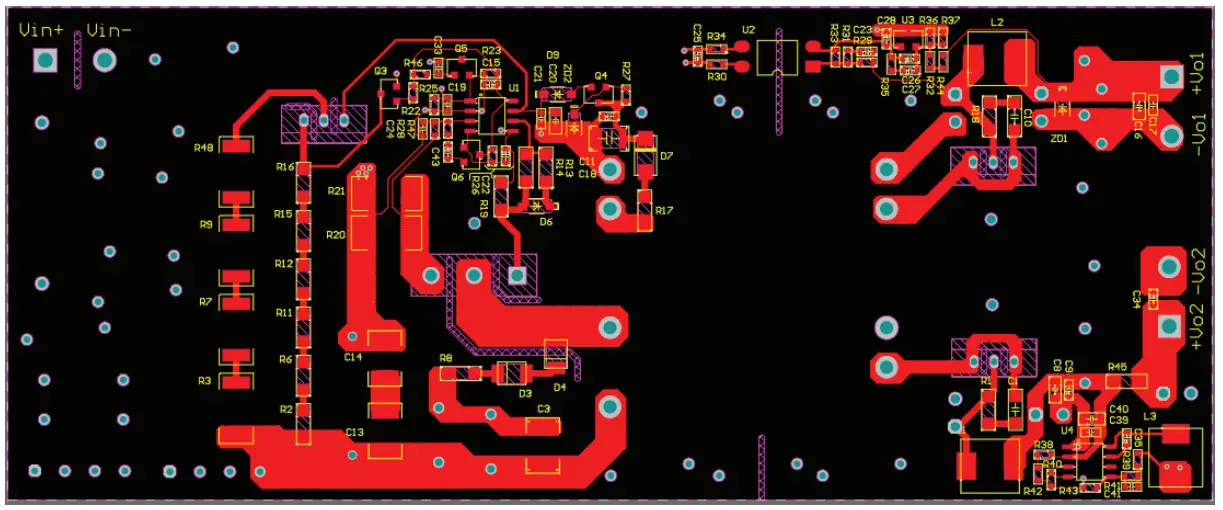 Figure 2-6. PCB Layout Design—Bottom Layer Copper and Bottom Side Component Placement
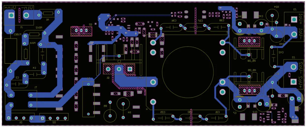
Bill Of Materials (BOM)
The following table lists BOM of the evaluation board.
Table 3-1. BOM of the Evaluation Board
| Type | Ratings/Part Number | Designator | Footprint | Description | Quantity |
|
Capacitor |
3.9 nF/630V | C3 | 1812 | TDK, ‘X7R, ±10% | 1 |
| 100 nF/630V | C13, C14 | 1812 | TDK, ‘X7R, ±10% | 2 | |
| 100 μF/35V | C7, C12, C32 | C 8*11-3.5 | AIHUA | 3 | |
| 220 μF/35V | C44, C45 | C 8*11-3.5 | AIHUA | 2 | |
| 1 μF | C8, C11, C16 | C0603 | TDK, ‘X7R, ±10%, 35V | 3 | |
| 100 nF | C9, C15, C17, C21 | C0603 | TDK, ‘X7R, ±10%, 35V | 4 | |
| 10 nF | C19 | C0603 | TDK, ‘X7R, ±10%, 35V | 1 | |
| 1 nF | C22 | C0603 | TDK, ‘X7R, ±10%, 35V | 1 | |
| 100 nF | C23 | C0603 | TDK, ‘X7R, ±10%, 35V | 1 | |
| 200 pF | C24, C34, C35, C39, C41 | C0603 | TDK, ‘X7R, ±10%, 35V | 5 | |
| 22 nF | C25 | C0603 | TDK, ‘X7R, ±10%, 35V | 1 | |
| NC | C26, C28, C33, C43 | C0603 | TDK, ‘X7R, ±10%, 35V | 4 | |
| 10 nF | C27 | C0603 | TDK, ‘X7R, ±10%, 35V | 1 | |
| 10 μF | C20, C40 | C0805 | TDK, ‘X7R, ±10%, 35V | 2 | |
| 100 pF | C1, C10 | C1206 | TDK, ‘X7R, ±10%, 35V | 2 | |
| 10 μF | C18 | C1210 | TDK, ‘X7R, ±10%, 35V | 1 | |
| 3 μF/1100V | C6 | C-18*6-15P | HJC | 1 | |
| 2.2 μF/450V | C2, C4, C5 | CY-222-4.5X14 | ±10% | 3 | |
| 2200 pF | C29, C30, C31, C36, C37, C38, C42 | CY-222-4.5X14 | KEMET | 7 |
| ………..continued | |||||
| Type | Ratings/Part Number | Designator | Footprint | Description | Quantity |
|
Resistor |
510 kΩ | R22, R38 | R0603 | YAGEO, ±1% | 2 |
| 5.1 kΩ | R23 | R0603 | YAGEO, ±1% | 1 | |
| NC | R25, R37, R46, R47 | R0603 | YAGEO, ±1% | 4 | |
| 23 kΩ | R26 | R0603 | YAGEO, ±1% | 1 | |
| 10 kΩ | R27 | R0603 | YAGEO, ±1% | 1 | |
| 1 kΩ | R28, R29, R33 | R0603 | YAGEO, ±1% | 3 | |
| 0Ω | R30, R34, R39 | R0603 | YAGEO, ±1% | 3 | |
| 5.6 kΩ | R31 | R0603 | YAGEO, ±1% | 1 | |
| 21.5 kΩ | R32 | R0603 | YAGEO, ±1% | 1 | |
| 14.3 kΩ | R35 | R0603 | YAGEO, ±1% | 1 | |
| 2.43 kΩ | R36 | R0603 | YAGEO, ±1% | 1 | |
| 68 kΩ | R40, R42 | R0603 | YAGEO, ±1% | 2 | |
| 230 kΩ | R41 | R0603 | YAGEO, ±1% | 1 | |
| 20 kΩ | R43 | R0603 | YAGEO, ±1% | 1 | |
| 51Ω | R44 | R0603 | YAGEO, ±1% | 1 | |
| 2.2Ω | R13 | R0805 | YAGEO, ±1% | 2 | |
| 10Ω | R14 | R0805 | YAGEO, ±1% | 2 | |
| NC | R45 | R1206 | YAGEO, ±1% | 1 | |
| 51Ω | R1 | R1206 | YAGEO, ±1% | 1 | |
| 1.5 MΩ | R2, R6, R11, R12, R15, R16 | R1206 | YAGEO, ±1% | 6 | |
| 0Ω | R8 | R1206 | YAGEO, ±1% | 1 | |
| NC | R10 | R-6.8-LS | YAGEO, ±1% | 1 | |
| 10Ω | R17 | R1206 | YAGEO, ±1% | 1 | |
| 33Ω | R18 | R1206 | YAGEO, ±1% | 1 | |
| 10 kΩ | R19 | R1206 | YAGEO, ±1% | 1 | |
| 150 kΩ | R3, R7, R9, R48 | R2512 | YAGEO, ±1% | 4 | |
| 1Ω | R20, R21 | R2512 | YAGEO, ±1% | 2 | |
| 68 kΩ/2W | R4, R5 | R-6.8-LS | YAGEO, ±1% | 2 | |
| 200Ω/5W | R24, R49 | R-6.8-LS | YAGEO, ±1% | 2 | |
|
Diode |
ES1D | D7 | SMA | ON, ST | 1 |
| RS1M | D3, D4 | SMB | ON, ST | 2 | |
| SS14 | D6, D9 | SOD123 | ON, ST | 2 | |
| 27V | ZD1 | SOD123 | UMZ27K | 1 | |
| 18V | ZD2 | SOD123 | BZT52C18 | 1 | |
| D4UB100 | D1, D2 | D3K | YJ | 2 | |
| DSA20C200PB | D5, D8 | TO-220AB | Littelfuse | 2 | |
| ………..continued | |||||
| Type | Ratings/Part Number | Designator | Footprint | Description | Quantity |
|
Integrated Circuit (IC) |
MIC38C44 | U1 | SOIC8 | Microchip | 1 |
| MCP16311 | U4 | SOIC8 | Microchip | 1 | |
| 817A | U2 | OPTO-SMT | TI | 1 | |
| TL431 | U3 | SOT23 | TI | 1 | |
|
NPN transistor |
STN0214 | Q2 | SOT223 | ST | 1 |
| MMBT2222A | Q3, Q4, Q6 | SOT23 | ON, ST | 3 | |
| PNP transistor | MMBT4403 | Q5 | SOT23 | ON, ST | 1 |
| MOSFET | MSC750SMA170B | Q1 | TO-247 | MC | 1 |
| Fuse | FUSE | FUSE1 | AXIAL0.8 | Littelfuse | 1 |
| Header | Header 2H | J1, J2, J3 | HDR1X2-7.5 | TE | 3 |
|
Heat sink |
Heat sink | HS_D5, HS_D8 | HS-TO220-1 | — | 2 |
| Heat sink | HS_Q1 | HS-TO247-1 | — | 1 | |
|
Inductance |
2.2 μH | L1, L2 | IN-L | 3A | 2 |
| 10 μH | L3 | IN-L | 2A | 1 | |
| 70 mΩ/2A | T1 | LL | PDMCAT1386-472ML | 1 | |
| MOV | — | MOV1, MOV2 | MOV | Placeholder | 2 |
| Negative Temperature Coefficient (NTC) |
NTC |
N1 |
NTC |
Placeholder |
1 |
| Transformer | Trans BB | T2 | PQ3528 | — | 1 |
Quick Startup and Test Procedure
Perform the following steps to quickly boot up and test the evaluation board:
- Visually inspect any damage to the board and the components. Examine for bending, breaking, or a change in shape.
- Connect the DC input to the DC power supply and the two DC outputs to passive or electronic loads, making sure to match the positive/negative connections.
- Connect all the measurement equipment, such as oscilloscope probes and Digital Multimeter (DMM).
- Start with a DC input of 10V/0.1A and monitor the DC source current. Make sure the DC source current is close to 0 to ensure there is no short circuit in the system. If the DC source current is 0.1A, there is a short circuit in the input. Stop the system and look for problems.
- Set the DC source to 250V/0.5A for normal testing, and the outputs setups after 0.5s.
Experimental Testing Results
This chapter describes the results of tests performed on SiC MOSFET.
5.1 Operation Waveforms
The converter operates at Continuous Conduction Mode (CCM) with a 250V input voltage at 50% and 100% load and at Discontinuous Conduction Mode (DCM) with a 1 kV input voltage at 50% and 100% load. The drain-to-source peak voltage on the MOSFET is well below the 1.7 kV device rated voltage.
The RCD circuit well clamps the device drain-to-source voltage, but there is still some VDS ringing after device turn-off due to the relatively large leakage inductance of the transformer. Because of the relatively large gate resistance and good PCB layout design, the gate voltage has small voltage overshoot and undershoot during device switching transient. The gate signal VGS is clean during both the turn-on and turn-off transients. The measured gate voltage on the device is 16.5V, and works well with 0V gate voltage during turn-off.
The following figures show the operation waveforms for SiC MOSFET at different input voltages and steady-state output power levels.
Note: In the following operation waveforms, drain-to-source voltage (VDS) is blue, gate-to-source voltage (VGS) is red, and device current (IDS) is green.
Figure 5-1. Operation Waveform at Vin = 250V and 50% Load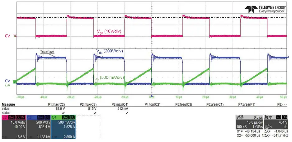 Figure 5-2. Operation Waveform at Vin = 250V and 100% Load
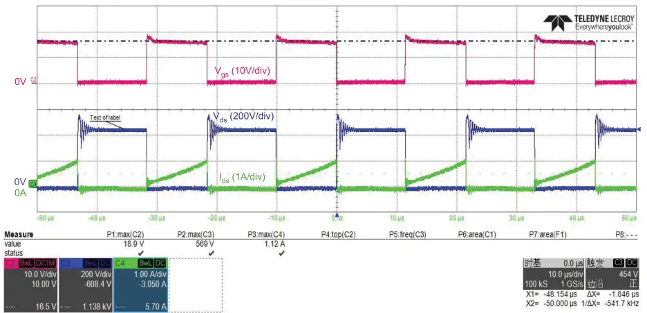 Figure 5-3. Operation Waveform at Vin = 1000V and 50% Load
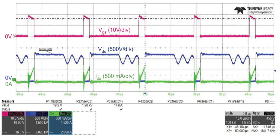 Figure 5-4. Operation Waveform at Vin = 1000V and 100% Load
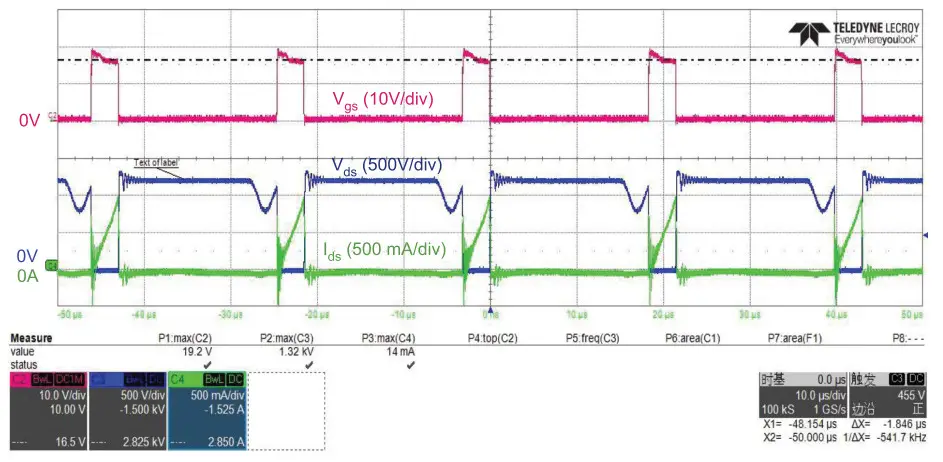 5.2 Thermal Performance
With only a small heatsink and no fan cooling, the primary side MOSFET temperature rise is only 25.8 °C in the worst case, demonstrating that the MOSFETs can process much higher power and that the heatsink is not required in some applications. The maximum temperature rise of the power transformer is 37.5 °C, which validates its effectiveness. At full load, the highest temperature rise (47.6 °C) is measured on the rectifier diode of output 1. The output diodes are connected to a small heatsink, and natural convection cooling is used. The results validate the design effectiveness and show that the temperature rise of all the major components in the converter design is relatively low due to the small heatsink and natural convection cooling.
The following figure shows the thermal performance of the converter at full load under different input voltage conditions.
Figure 5-5. Temperature Measurement Results Vout2 Diode, SiC FET, and Input Diode
at Vin = 250V Power Transformer at Vin = 250V Vout1 Diode at Vin = 250V 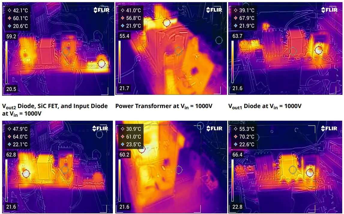 5.3 Power Loss and Efficiency
The switching loss of the converter increases significantly with high input voltage, so the efficiency at 1 kV is lower than the efficiency at 400V and 250V. Above 25% load, the converter efficiency is more than 80% for 250V and 400V input voltages, with a peak efficiency of 89% at 100% load and 400Vinput voltage.
The following figure shows the efficiency measurement results for the demo converter at different input voltage and load conditions.
Figure 5-6. Measured Efficiency vs. Output Power Load Under Different Input Voltage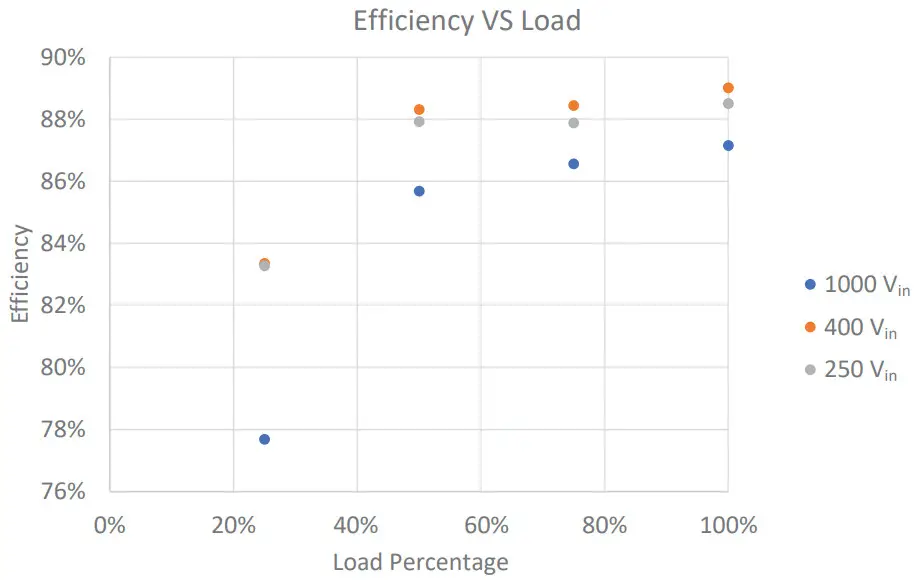 More test results are available, including the steady state output voltage ripple. For more information on load and line regulations, start-up time, hold-up time, and short circuit protection results for various working conditions, contact the Microchip technical support team.
Reference Documents
The following document is referred in this user guide:
- MIC38C42/43/44/45 BiCMOS Current-Mode PWM Controllers Data Sheet
Revision History
The revision history describes the changes that were implemented in the document. The changes are listed by revision, starting with the most current publication.
| Revision | Date | Description |
| B | 06/2023 | Replaced HV SiC MOSFETs with HV silicon MOSFETs and lower rated voltage SiC MOSFETs with lower rated voltage silicon MOSFETs in Introduction. |
| A | 02/2023 | Initial revision |
Microchip Information
The Microchip Website
Microchip provides online support via our website at www.microchip.com/. This website is used to make files and information easily available to customers. Some of the content available includes:
- Product Support – Data sheets and errata, application notes and sample programs, design resources, user’s guides and hardware support documents, latest software releases and archived software
- General Technical Support – Frequently Asked Questions (FAQs), technical support requests, online discussion groups, Microchip design partner program member listing
- Business of Microchip – Product selector and ordering guides, latest Microchip press releases, listing of seminars and events, listings of Microchip sales offices, distributors and factory representatives
Product Change Notification Service
Microchip’s product change notification service helps keep customers current on Microchip products. Subscribers will receive email notification whenever there are changes, updates, revisions or errata related to a specified product family or development tool of interest.
To register, go to www.microchip.com/pcn and follow the registration instructions.
Customer Support
Users of Microchip products can receive assistance through several channels:
- Distributor or Representative
- Local Sales Office
- Embedded Solutions Engineer (ESE)
- Technical Support
Customers should contact their distributor, representative or ESE for support. Local sales offices are also available to help customers. A listing of sales offices and locations is included in this document.
Technical support is available through the website at: www.microchip.com/support
Microchip Devices Code Protection Feature
Note the following details of the code protection feature on Microchip products:
- Microchip products meet the specifications contained in their particular Microchip Data Sheet.
- Microchip believes that its family of products is secure when used in the intended manner, within operating specifications, and under normal conditions.
- Microchip values and aggressively protects its intellectual property rights. Attempts to breach the code protection features of Microchip product is strictly prohibited and may violate the Digital Millennium Copyright Act.
- Neither Microchip nor any other semiconductor manufacturer can guarantee the security of its code. Code protection does not mean that we are guaranteeing the product is “unbreakable”. Code protection is constantly evolving. Microchip is committed to continuously improving the code protection features of our products.
Legal Notice
This publication and the information herein may be used only with Microchip products, including to design, test, and integrate Microchip products with your application. Use of this information in any other manner violates these terms. Information regarding device applications is provided only for your convenience and may be superseded by updates. It is your responsibility to ensure that your application meets with your specifications. Contact your local Microchip sales office for additional support or, obtain additional support at www.microchip.com/en-us/support/design-help/clientsupport-services.
THIS INFORMATION IS PROVIDED BY MICROCHIP “AS IS”. MICROCHIP MAKES NO REPRESENTATIONS OR WARRANTIES OF ANY KIND WHETHER EXPRESS OR IMPLIED, WRITTEN OR ORAL, STATUTORY OR OTHERWISE, RELATED TO THE INFORMATION INCLUDING BUT NOT LIMITED TO ANY IMPLIED WARRANTIES OF NON-INFRINGEMENT, MERCHANTABILITY, AND FITNESS FOR A PARTICULAR PURPOSE, OR WARRANTIES RELATED TO ITS CONDITION, QUALITY, OR PERFORMANCE.
IN NO EVENT WILL MICROCHIP BE LIABLE FOR ANY INDIRECT, SPECIAL, PUNITIVE, INCIDENTAL, OR CONSEQUENTIAL LOSS, DAMAGE, COST, OR EXPENSE OF ANY KIND WHATSOEVER RELATED TO THE INFORMATION OR ITS USE, HOWEVER CAUSED, EVEN IF MICROCHIP HAS BEEN ADVISED OF THE POSSIBILITY OR THE DAMAGES ARE FORESEEABLE. TO THE FULLEST EXTENT ALLOWED BY LAW, MICROCHIP’S TOTAL LIABILITY ON ALL CLAIMS IN ANY WAY RELATED TO THE INFORMATION OR ITS USE WILL NOT EXCEED THE AMOUNT OF FEES, IF ANY, THAT YOU HAVE PAID DIRECTLY TO MICROCHIP FOR THE INFORMATION.
Use of Microchip devices in life support and/or safety applications is entirely at the buyer’s risk, and the buyer agrees to defend, indemnify and hold harmless Microchip from any and all damages, claims, suits, or expenses resulting from such use. No licenses are conveyed, implicitly or otherwise, under any Microchip intellectual property rights unless otherwise stated.
Trademarks
The Microchip name and logo, the Microchip logo, Adaptec, AVR, AVR logo, AVR Freaks, BesTime, BitCloud, CryptoMemory, CryptoRF, dsPIC, flexPWR, HELDO, IGLOO, JukeBlox, KeeLoq, Kleer, LANCheck, LinkMD, maXStylus, maXTouch, MediaLB, megaAVR, Microsemi, Microsemi logo, MOST, MOST logo, MPLAB, OptoLyzer, PIC, picoPower, PICSTART, PIC32 logo, PolarFire, Prochip Designer, QTouch, SAM-BA, SenGenuity, SpyNIC, SST, SST Logo, SuperFlash, Symmetricom, SyncServer, Tachyon, TimeSource, tinyAVR, UNI/O, Vectron, and XMEGA are registered trademarks of Microchip Technology Incorporated in the U.S.A. and other countries.
AgileSwitch, APT, ClockWorks, The Embedded Control Solutions Company, EtherSynch, Flashtec, Hyper Speed Control, HyperLight Load, Libero, motorBench, mTouch, Powermite 3, Precision Edge, ProASIC, ProASIC Plus, ProASIC Plus logo, Quiet- Wire, SmartFusion, SyncWorld, Temux, TimeCesium, TimeHub, TimePictra, TimeProvider, TrueTime, and ZL are registered trademarks of Microchip Technology Incorporated in the U.S.A.
Adjacent Key Suppression, AKS, Analog-for-the-Digital Age, Any Capacitor, AnyIn, AnyOut, Augmented Switching, BlueSky, BodyCom, Clockstudio, CodeGuard, CryptoAuthentication, CryptoAutomotive, CryptoCompanion, CryptoController, dsPICDEM, dsPICDEM.net, Dynamic Average Matching, DAM, ECAN, Espresso T1S, EtherGREEN, GridTime, IdealBridge, In-Circuit Serial Programming, ICSP, INICnet, Intelligent Paralleling, IntelliMOS, Inter-Chip Connectivity, JitterBlocker, Knob-on-Display, KoD, maxCrypto, maxView, memBrain, Mindi, MiWi, MPASM, MPF, MPLAB Certified logo, MPLIB, MPLINK, MultiTRAK, NetDetach, Omniscient Code Generation, PICDEM, PICDEM.net, PICkit, PICtail, PowerSmart, PureSilicon, QMatrix, REAL ICE, Ripple Blocker, RTAX, RTG4, SAMICE, Serial Quad I/O, simpleMAP, SimpliPHY, SmartBuffer, SmartHLS, SMART-I.S., storClad, SQI, SuperSwitcher, SuperSwitcher II, Switchtec, SynchroPHY, Total Endurance, Trusted Time, TSHARC, USBCheck, VariSense, VectorBlox, VeriPHY, ViewSpan, WiperLock, XpressConnect, and ZENA are trademarks of Microchip Technology Incorporated in the U.S.A. and other countries.
SQTP is a service mark of Microchip Technology Incorporated in the U.S.A.
The Adaptec logo, Frequency on Demand, Silicon Storage Technology, and Symmcom are registered trademarks of Microchip Technology Inc. in other countries.
GestIC is a registered trademark of Microchip Technology Germany II GmbH & Co. KG, a subsidiary of Microchip Technology Inc., in other countries.
All other trademarks mentioned herein are property of their respective companies.
©2023, Microchip Technology Incorporated and its subsidiaries. All Rights Reserved. ISBN: 978-1-6683-2697-8
Quality Management System
For information regarding Microchip’s Quality Management Systems, please visit www.microchip.com/quality.
Worldwide Sales and Service
| AMERICAS | ASIA/PACIFIC | ASIA/PACIFIC | EUROPE |
| Corporate Office 2355 West Chandler Blvd. Chandler, AZ 85224-6199 Tel: 480-792-7200 Fax: 480-792-7277 Technical Support: www.microchip.com/support Web Address: www.microchip.com Atlanta Duluth, GA Tel: 678-957-9614 Fax: 678-957-1455 Austin, TX Tel: 512-257-3370 Boston Westborough, MA Tel: 774-760-0087 Fax: 774-760-0088 Chicago Itasca, IL Tel: 630-285-0071 Fax: 630-285-0075 Dallas Addison, TX Tel: 972-818-7423 Fax: 972-818-2924 Detroit Novi, MI Tel: 248-848-4000 Houston, TX Tel: 281-894-5983 Indianapolis Noblesville, IN Tel: 317-773-8323 Fax: 317-773-5453 Tel: 317-536-2380 Los Angeles Mission Viejo, CA Tel: 949-462-9523 Fax: 949-462-9608 Tel: 951-273-7800 Raleigh, NC Tel: 919-844-7510 New York, NY Tel: 631-435-6000 San Jose, CA Tel: 408-735-9110 Tel: 408-436-4270 Canada – Toronto Tel: 905-695-1980 Fax: 905-695-2078 |
Australia – Sydney Tel: 61-2-9868-6733 China – Beijing Tel: 86-10-8569-7000 China – Chengdu Tel: 86-28-8665-5511 China – Chongqing Tel: 86-23-8980-9588 China – Dongguan Tel: 86-769-8702-9880 China – Guangzhou Tel: 86-20-8755-8029 China – Hangzhou Tel: 86-571-8792-8115 China – Hong Kong SAR Tel: 852-2943-5100 China – Nanjing Tel: 86-25-8473-2460 China – Qingdao Tel: 86-532-8502-7355 China – Shanghai Tel: 86-21-3326-8000 China – Shenyang Tel: 86-24-2334-2829 China – Shenzhen Tel: 86-755-8864-2200 China – Suzhou Tel: 86-186-6233-1526 China – Wuhan Tel: 86-27-5980-5300 China – Xian Tel: 86-29-8833-7252 China – Xiamen Tel: 86-592-2388138 China – Zhuhai Tel: 86-756-3210040 |
India – Bangalore Tel: 91-80-3090-4444 India – New Delhi Tel: 91-11-4160-8631 India – Pune Tel: 91-20-4121-0141 Japan – Osaka Tel: 81-6-6152-7160 Japan – Tokyo Tel: 81-3-6880- 3770 Korea – Daegu Tel: 82-53-744-4301 Korea – Seoul Tel: 82-2-554-7200 Malaysia – Kuala Lumpur Tel: 60-3-7651-7906 Malaysia – Penang Tel: 60-4-227-8870 Philippines – Manila Tel: 63-2-634-9065 Singapore Tel: 65-6334-8870 Taiwan – Hsin Chu Tel: 886-3-577-8366 Taiwan – Kaohsiung Tel: 886-7-213-7830 Taiwan – Taipei Tel: 886-2-2508-8600 Thailand – Bangkok Tel: 66-2-694-1351 Vietnam – Ho Chi Minh Tel: 84-28-5448-2100 |
Austria – Wels Tel: 43-7242-2244-39 Fax: 43-7242-2244-393 Denmark – Copenhagen Tel: 45-4485-5910 Fax: 45-4485-2829 Finland – Espoo Tel: 358-9-4520-820 France – Paris Tel: 33-1-69-53-63-20 Fax: 33-1-69-30-90-79 Germany – Garching Tel: 49-8931-9700 Germany – Haan Tel: 49-2129-3766400 Germany – Heilbronn Tel: 49-7131-72400 Germany – Karlsruhe Tel: 49-721-625370 Germany – Munich Tel: 49-89-627-144-0 Fax: 49-89-627-144-44 Germany – Rosenheim Tel: 49-8031-354-560 Israel – Ra’anana Tel: 972-9-744-7705 Italy – Milan Tel: 39-0331-742611 Fax: 39-0331-466781 Italy – Padova Tel: 39-049-7625286 Netherlands – Drunen Tel: 31-416-690399 Fax: 31-416-690340 Norway – Trondheim Tel: 47-72884388 Poland – Warsaw Tel: 48-22-3325737 Romania – Bucharest Tel: 40-21-407-87-50 Spain – Madrid Tel: 34-91-708-08-90 Fax: 34-91-708-08-91 Sweden – Gothenberg Tel: 46-31-704-60-40 Sweden – Stockholm Tel: 46-8-5090-4654 UK – Wokingham Tel: 44-118-921-5800 Fax: 44-118-921-5820 |
User Guide
DS50003498B – 25
© 2023 Microchip Technology Inc. and its subsidiaries